Back to Journals » International Journal of Nanomedicine » Volume 15
Flexible and Transparent Artificial Synapse Devices Based on Thin-Film Transistors with Nanometer Thickness
Authors Dai C, Huo C, Qi S, Dai M ![]() , Webster T
, Webster T ![]() , Xiao H
, Xiao H
Received 16 June 2020
Accepted for publication 12 September 2020
Published 20 October 2020 Volume 2020:15 Pages 8037—8043
DOI https://doi.org/10.2147/IJN.S267536
Checked for plagiarism Yes
Review by Single anonymous peer review
Peer reviewer comments 3
Editor who approved publication: Prof. Dr. Anderson Oliveira Lobo
Chaoqi Dai, 1, 2,* Changhe Huo, 2,* Shaocheng Qi, 2,* Mingzhi Dai, 2, 3 Thomas Webster, 4 Han Xiao 1
1College of Materials Science and Engineering, Kunming University of Science and Technology, Kunming 650093, People’s Republic of China; 2Ningbo Institute of Materials Technology and Engineering, Chinese Academy of Sciences, Ningbo 315201, People’s Republic of China; 3Center of Materials Science and Optoelectronics Engineering, University of Chinese Academy of Sciences, Beijing 100049, People’s Republic of China; 4Department of Chemical Engineering, Northeastern University, MA, Boston 02115, USA
*These authors contributed equally to this work
Correspondence: Mingzhi Dai
Ningbo Institute of Materials Technology and Engineering, Chinese Academy of Sciences, Ningbo 315201, People’s Republic of China
Tel +86 151 5831 3993
Email [email protected]
Thomas Webster
Department of Chemical Engineering, Northeastern University, Boston, MA 02115, USA
Tel +1-617-373-6585
Email [email protected]
Background: Artificial synaptic behaviors are necessary to investigate and implement since they are considered to be a new computing mechanism for the analysis of complex brain information. However, flexible and transparent artificial synapse devices based on thin-film transistors (TFTs) still need further research.
Purpose: To study the application of flexible and transparent thin-film transistors with nanometer thickness on artificial synapses.
Materials and Methods: Here, we report the design and fabrication of flexible and transparent artificial synapse devices based on TFTs with polyethylene terephthalate (PET) as the flexible substrate, indium tin oxide (ITO) as the gate and a polyvinyl alcohol (PVA) grid insulating layer as the gate insulation layer at room temperature.
Results: The charge and discharge of the carriers in the flexible and transparent thin-film transistors with nanometer thickness can be used for artificial synaptic behavior.
Conclusion: In summary, flexible and transparent thin-film transistors with nanometer thickness can be used as pressure and temperature sensors. Besides, inherent charge transfer characteristics of indium gallium zinc oxide semiconductors have been employed to study the biological synapse-like behaviors, including synaptic plasticity, excitatory postsynaptic current (EPSC), paired-pulse facilitation (PPF), and long-term memory (LTM). More precisely, the spike rate plasticity (SRDP), one representative synaptic plasticity, has been demonstrated. Such TFTs are interesting for building future neuromorphic systems and provide a possibility to act as fundamental blocks for neuromorphic system applications.
Keywords: flexible, transparent, TFTs, thin-film transistors, artificial synapse devices, EPSC, excitatory post-synaptic current, PPF, paired-pulse facilitation
Corrigendum for this paper has been published
Introduction
In recent years, amorphous oxide semiconductor (AOS) devices have attracted much attention. A representative AOS material is In-Ga-Zn-O (IGZO) which has been one of the most popular AOS materials since it was first published in 2004.1 They have some attractive properties, including transparency, flexibility, relatively low-cost fabrication and low-temperature processing at no higher than 200 °C. TFTs can be used as pressure and temperature sensors.2,3 TFTs are used in many ways and artificial synapse devices based on TFTs have been extensively studied, however, flexible and transparent artificial synapses based on nano TFTs have not been researched as much despite their promise in numerous applications. Synapse is the functional unit in the brain, and it connects the presynaptic and postsynaptic neurons.4 In biological synapses, action potentials reach the pre-synapse, promote the release of the neurotransmitter, and cause excitatory postsynaptic potential (EPSP).5 In the artificial synaptic device mentioned in the manuscript, a voltage is applied to the gate electrode to simulate the action potential, and the change of the channel current is to simulate the excitatory postsynaptic current. Therefore, the presynaptic stimulation is the pulse applied to the gate electrode.6,7
For example, neurosynaptic behaviors are the basis of our learning, memory, and information processing. Artificial synaptic devices based on flexible TFTs can mimic biological synaptic behaviors like our brain and be useful for a number of applications.8 Therefore, artificial synapse devices are worthy of further study. The biological synapse-like behaviors include information memory and possessing, which are triggered by the inflow dynamics of ion transport. Artificial flexible organic synaptic transistors capable of concurrently exhibiting signal transmission and learning functions were verified using a C60/poly (methyl methacrylate) (PMMA) hybrid layer.9 Photonic non-volatile memory devices with hybrid polymer/UC nanocrystal composite materials as the active layer have been confirmed.10
In this work, the flexible and transparent artificial synapse devices based on TFTs with PET as the flexible substrate, ITO as the gate, and PVA as the gate insulation layer were made and showed some representative synaptic characteristics. The device shows good synaptic plasticity. Some biological synapse-like behaviors are mimicked in this paper, for instance, excitatory postsynaptic current (EPSC),11–13 paired-pulse facilitation (PPF) and long-term memory (LTM) demonstrating much promise for these materials in many fields.14–17 As far as we know, few previous publications are on such a standard thin-film transistor structure, which is based on PVA insulators and IGZO semiconductors. At the same time, the design here has a combination of artificial synapse functions and temperature sensor characteristics.
Materials and Methods
As shown in Figure 1A and B, the bottom-gate top-contact structure was used for the design of the present flexible and transparent TFTs. The TFTs employed PET as the flexible substrate, ITO as the bottom gate, and PVA as the gate insulation layer. For the deposition of the gate insulation layer, the processing steps were as follows. First, a 10 wt% PVA solution was prepared by magnetic stirring and heating in ambient air. The solution used for the spin-coating of the PVA insulator layer was deionized water. PVA acted as the insulating layer on the ITO gate and was added via a spin coating method at a speed of 200 rpm for 3 s and 2000 rpm for 20 s. Afterward, it was heated at 90 °C for 30 minutes. The IGZO films acted as the semiconductor layer with a thickness of 35 nm or so and were deposited on the insulating layer by radio-frequency (RF) magnetron sputtering. The RF magnetron sputtering instrument was produced by Shenyang Scientific Instrument Co., Ltd., Chinese Academy of Sciences. The IGZO films were formed by using an IGZO target and a shadow mask (size: 600 μm × 800 μm). The composition of the IGZO sputtering target was the molecular ratio of In2O3: Ga2O3: ZnO = 1: 1: 1. The deposition conditions included an RF power of 100 W, a pressure of 0.5 Pa, Ar gas flow rate of 14 sccm and sputtering time of 5 min. In Figure 1C and D, for the source and drain electrodes, a ~100 nm-thick top ITO electrode layer was deposited on the IGZO channel layer and formed a covering in contact with the IGZO channel layer. The deposition conditions were the same as IGZO except the sputtering time was about 15 min. The source and drain electrodes could also be deposited by RF magnetron sputtering with a shadow mask (size: 150 μm × 1000 μm). Figure 1C is the SEM image, obtained from FEI Quanta 250 FEG produced by Keesida Co., LTD. The artificial synapse behavior of the devices was measured and investigated using a Keithley 4200 semiconductor analyzer.
 |
Figure 1 Thin-film transistor-based synapse device. (A) Three-dimensional structure of the single thin film transistor. (B) Cross-section structure of the single thin film transistor. (C) SEM top image of a single device and (D) Flexible transparent single device in an enlarged image. |
Results and Discussion
Figure 2A shows the transfer characteristic curve, where VDS is 1.1 V, the gate voltage VGS is scanned from  2 V to 3 V, and the voltage sweeping rate is 0.1 V. It can be calculated that ION/IOFF = 4.58×10⁶ from the data in Figure 2A. The carrier charges gradually increase on the interface between the dielectrics and IGZO semiconductor channel as the voltage increases, and then the current is generated between the source and the drain electrodes. As shown in the Figure 2B, the VDS sweeps from 0 V to 2 V, and the gate voltage VGS increases from 0.35 V to 2 V with a step of 0.55 V. When VDS is consistent, the value of IDS increases when VGS increases, so the black line at the bottom represents VGS = 0.35 V. As can be seen from the figure, when the VDS is low, the device has an obvious linear region. When the VDS is high, the device shows good saturation current characteristics. The device can be used as temperature sensors, too. In Figure 2C, the transfer curves are measured when the drain-source voltage VDS = 1 V. When the temperature increases, the curves have a positive shift, this is the key to prove the device can work as a temperature sensor. The continuous modulation of the synaptic weight can be defined as synaptic plasticity.18 Therefore, the synapse can perform learning and memory functions. Spiking-rate dependent plasticity (SRDP) belongs to the class of synaptic plasticity. It is important to realize this in artificial synapses. Figure 2D shows the experiment of the spiking-rate dependent plasticity (SRDP). The drain-source voltage is 1.5 V and the gate-source voltage is 2 V. Here, the pulse width and pulse interval remain the same. When the pulse interval is 0.02 s, 0.03 s, and 0.04 s, the corresponding amplitudes of the drain current are 12 µA, 8 µA, and 6 µA, respectively, which decrease sequentially. The synaptic response is related to the frequency and can prove the learning rule of SRDP. Due to the change of the frequency, the synapse weight between neurons changes. In other words, presynaptic spikes with high frequency will lead to potentiation, whereas presynaptic spikes with low frequency will result in depression.
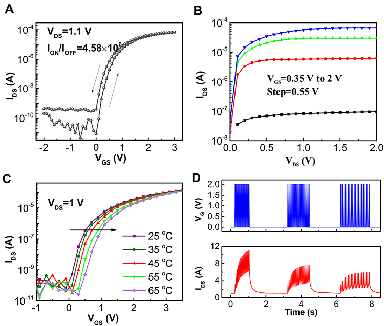 |
Figure 2 The biological synapse-like transfer and output characteristic curves of the thin film transistors (TFTs). (A) Transfer characteristic curves. (B) Output characteristic curves. (C) Transfer curves measured by different temperatures and (D) The spiking-rate-dependent plasticity experiment. |
Figure 3A shows a simplified biological dendritic synapse. A synapse is a connection between two neurons in the brain which allow neurons to transmit electrical or chemical signals to another neuron.19 The local magnification shows that synaptic plasticity is regulated by the migration of neurotransmitters, which are triggered by ion exchange at the membrane and synaptic junctions when the stimulation signal arrives.20,21 When the nerve impulse reaches the presynaptic region, the voltage-gated ion channel is opened, and then the ions migrate through the channel, causing the neurotransmitter to release into the synaptic spaces. The neurotransmitters then bind to the postsynaptic receptors to complete transmission of the information. Therefore, the ion transport plays a key role in regulating synaptic weight and transport information. As shown in Figure 3B, the gate electrode of the flexible and transparent TFTs corresponds to the presynaptic region, the source/drain electrode as the postsynaptic region, the IGZO channel as the synaptic cleft, and the carriers in the channel as the ions in the neural synapse.
 |
Figure 3 (A) Structure of synapses, including the synaptic cleft; presynaptic and postsynaptic neuron parts and (B) Corresponding relationship between biological synapses and TFTs. |
Figure 4A shows the measurement condition for the Keithley 4200 with probe pulses. One or more pulses are applied to the gate electrode and then the current at the drain is read. Figure 4B shows the EPSC of the artificial synaptic transistor and during the EPSC measurement, a constant drain voltage of 1.5 V was applied. The EPSC was triggered by a presynaptic spike (9.0 V, 1.0 s) on the ITO bottom gate electrode. The presynaptic spike triggers an EPSC current with a peak value of ~2.5×10⁻⁶ A and at the end of the spike, it gradually reduced to the initial current. When the voltage increases and the transistor is in the over-threshold region, the channel can be seen as a capacitor. Voltage pulses with amplitudes 915 V can be regarded as the maximum voltage at which the capacitor discharges. When a positive presynaptic spike is applied on the bottom ITO gate electrode, the mobile carriers will migrate and accumulate at the interface between the dielectrics and the IGZO semiconductor channel. When the spike ends for a while, the accumulated carriers will gradually migrate back to their initial equilibrium position due to the concentration gradient.22 The postsynaptic parameters can influence the EPSC, and it can be found in our previous publications.11 The drain-source voltages can provide a range of post-spikes and influence the output current. The equation can be seen as follows:
where τ is the retention time, t0 is the time when the presynaptic spike finishes, I0 is the triggered maximum EPSC, and I∞ is the EPSC at the end of the presynaptic spike. τ is found to be voltage-dependent.
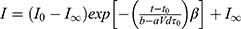
When the presynaptic neurons are stimulated by two consecutive pulses, the second peak triggered by the pulses is larger than the first peak. This phenomenon is called a paired-pulse boost (PPF), which plays an important role in visual and auditory signal processing.23 Here, we can imitate the phenomenon of the PPF in the artificial synaptic transistor. Figure 4C shows a PPF response in the flexible and transparent artificial synaptic transistor. Two successive identical pulses (15.0 V, 1.0 s) with an interval time of 2.8 s are applied to the ITO gate with a constant VD of 1.5 V. The values of the first EPSC (I1) and the second EPSC (I2) are respectively ~6.9×10⁻⁷ A and ~4.5×10⁻⁶ A, meanwhile, an EPSC gain (I2/I1) of ~6.5 times is obtained. At the end of the first spike, some of the activated carriers remain on the interface between the IGZO channel and the insulating layer before they return to their original position.17 Therefore, when the second peak is applied to the gate after the first spike with a small inter-spike interval, the values of the second EPSC (I2) is larger than the first EPSC (I1).
In the biological nervous system, some of the changes in synaptic connections can last for hours or even days. This phenomenon is known as the long-term memory (LTM), which is the basis for learning, memory and information processing.24 As shown in Figure 4D, ten sequential identical pulses (15.0 V, 1.0 s) with an interval time of 2.0 s are applied to the ITO gate with a constant VD of 1.5 V. Figure 4C shows the peaks progressively increase by the successive application of gate pulses and it lasts a long time after the end of the pulse. The LTM process is due to some of the carriers of the IGZO channel changing irreversibly under the continuous high gate pulses.25
 |
Figure 4 (A) The pulse measurement schematic diagram based on IGZO transistors. (B) The excitatory postsynaptic current (EPSC) plotted versus time. (C) A PPF response for the artificial synaptic transistor and (D) The EPSC response triggered by ten sequential gate pulses. |
Artificial synaptic behaviors are caused by charging and discharging of the moving carriers stimulated by the gate pulse as shown in Figure 5. Figure 5A shows that the carrier transport behavior during a period of the pulse could be divided into five stages: the basic voltage V1, the instantaneous rising voltage V2, the higher voltage V3, one instantaneous dropping voltage V4, and the last basic voltage V5. As shown in Figure 5B, at stage ①, when the V1 is applied, the mobile carriers are not attracted to the interface between the dielectrics and the IGZO semiconductor channel. At stage ②, when the V2 is applied to the gate, it increases instantaneously, and the mobile carriers at the interface between the IGZO channel and the insulating layer PVA gradually increase. Meanwhile, the functional groups such as In-O, Ga-O, and Zn-O can interact with metal ions and persist in the channel. At stage ③, when the gate voltage is kept at a higher voltage V3, more carriers remain at the interface between the dielectrics and the IGZO semiconductor channel. Stage ④ is just the opposite of stage ②. The accumulated mobile carriers at the interface between the dielectrics and the IGZO semiconductor channel are driven back into the source and the drain electrodes. The migration rate in stage ④ is slower than in stage ②, because, at stage ②, the free carriers move faster under pulse pressure, while at stage ④, free carriers diffuse slower back to the original position due to the concentration gradient.26 Stage ⑤ is the same as stage ①. When the gate voltage drops to V5, there are no carriers at the interface between the IGZO channel and the insulating layer and then the device returns to its initial state.27,28
 |
Figure 5 (A) Schematic diagram of the pre-synaptic spike applied to the gate electrode and (B) Overview of the voltage pulse profile and the corresponding discharge current in the TFTs with the IGZO channel. |
Conclusion
In summary, in this study, we have fabricated flexible and transparent artificial synapse transistors with PET as the flexible substrate and PVA as the dielectric layer, and its ION/IOFF ratio was 4.58×10⁶. The TFTs have a thickness on the order of nanometers. They can be used as temperature sensors and shows good spiking-rate dependent plasticity (SRDP). Furthermore, we succeeded in mimicking the biological synapse-like behaviors of EPSC, PPI, and LTM in the biological nervous system with artificial synaptic transistors. Although it cannot be used on a large scale at present, such artificial synaptic transistors provide a possibility to realize synaptic-like information processing and learning, and lay the foundation for the development of artificial intelligence.
Funding
This work was supported by the National Science and Technology Major Project of the Ministry of Science and Technology of China (Grant No. 2017YFB03031001), the National Natural Science Foundation of China (Grant No. 61574147), Zhejiang Provincial Natural Science Foundation for Distinguished Young Scholars (Grant No. LR 17F040002), the Instrument Developing Project of the Chinese Academy of Sciences (Grant No. YJKY YQ20180021), the Project of the National Natural Science Foundation for major research projects (Grant No. 91648109), and the Ningbo Natural Science Foundation of China (Grant No. 2018A610003).
Disclosure
The authors report no conflicts of interest in this work.
References
1. Nomura K, Ohta H, Takagi A, Kamiya T, Hirano M, Hosono H. Room-temperature fabrication of transparent flexible thin-film transistors using amorphous oxide semiconductors. Nature. 2004;432(7016):488–492. doi:10.1038/nature03090
2. Jeon S, Ahn SE, Song I, et al. Gated three-terminal device architecture to eliminate persistent photoconductivity in oxide semiconductor photosensor arrays. Nat Mater. 2015;11(4):301–305. doi:10.1038/nmat3256
3. Fortunato E, Barquinha P, Martins R. Oxide semiconductor thin-film transistors: a review of recent advances. Adv Mater. 2012;24(22):2945–2986. doi:10.1002/adma.201103228
4. Zhong Y-N, Wang T, Gao X, Xu J-L, Wang S-D. Synapse–like organic thin film memristors. Adv Func Mater. 2018;28:1800854. doi:10.1002/adfm.201800854
5. Wan H, Cao Y, Lo L-W, Zhao J, Sepulveda N, Wang C. Flexible carbon nanotube synaptic transistor for neurological electronic skin applications. ACS Nano. 2020;14:10402–10412. doi:10.1021/acsnano.0c04259
6. Yang J-T, Ge C, Du J-Y, et al. Artificial synapses emulated by an electrolyte-gated tungsten-oxide transistor. Adv Mater. 2018;30:1801548. doi:10.1002/adma.201801548
7. Wu C, Kim TW, Choi HY, Stricov DB, Yang JJ. Flexible three-dimensional artificial synapse networks with correlated learning and trainable memory capability. Nat Commun. 2017;8:752. doi:10.1038/s41467-017-00803-1
8. Brunel D, Anghel C, Kim DY, et al. Integrating multiple resistive memory devices on a single carbon nanotube. Adv Func Mater. 2013;23(45):5631–5637. doi:10.1002/adfm.201300775
9. Ren Y, Yang J‐Q, Zhou L, Mao J‐Y, Zhang S‐R. Gate‐tunable synaptic plasticity through controlled polarity of charge trapping in fullerene composites. Adv Func Mater. 2018;28(50):1805599. doi:10.1002/adfm.201805599
10. Zhou Y, Han ST, Chen X, Wang F, Tang YB, Roy VA. An upconverted photonic nonvolatile memory. Nat Commun. 2014;5:4720. doi:10.1038/ncomms5720
11. Dai M, Wang W, Wang P, Iqbal MZ, Annabi N, Amin N. Realization of tunable artificial synapse and memory based on amorphous oxide semiconductor transistor. Sci Rep. 2017;7(1):10997. doi:10.1038/s41598-017-04641-5
12. Lai Q, Zhang L, Li Z, Stickle WF, Williams RS, Chen Y. Ionic/electronic hybrid materials integrated in a synaptic transistor with signal processing and learning functions. Adv Mater. 2010;22(22):2448–2453. doi:10.1002/adma.201000282
13. Song J, Ampatzis K, Björnfors ER, El MA. Motor neurons control iocomotor circuit function retrogradely via gap junctions. Nature. 2016;529(7586):399–402. doi:10.1038/nature16497
14. Sengupta A, Roy K. Short-term plasticity and long-term potentiation in magnetic tunnel junctions: towards volatile synapses. Phys Rev Appl. 2016;5(2):024012. doi:10.1103/PhysRevApplied.5.024012
15. Chang T, Jo SH, Lu W. Short-term memory to long-term memory transition in a nanoscale memristor. ACS Nano. 2011;5(9):7669–7676. doi:10.1021/nn202983n
16. Ohno T, Hasegawa T, Tsuruoka T, Terabe K, Gimzewski JK, Aono M. Short-term plasticity and long-term potentiation mimicked in single inorganic synapses. Nat Mater. 2011;10(8):591–595. doi:10.1038/nmat3054
17. Lee M-S, Lee J-W, Kim C-H, Park B-G, Lee J-H. Implementation of short-term plasticity and long-term potentiation in a synapse using Si-based type of charge-trap memory. IEEE Trans Electron Devices. 2015;62(2):569–573. doi:10.1109/ted.2014.2378758
18. Xiao Z, Huang J. Energy-efficient hybrid perovskite memristors and synaptic devices. Adv Electron Mater. 2016;2:1600100. doi:10.1002/aelm.201600100
19. Schacter DL. Psychology.
20. Sheng J, He L, Zheng H, et al. Calcium-channel number critically influences synaptic strength and plasticity at the active zone. Nat Neurosci. 2012;15(7):998–1006. doi:10.1038/nn.3129
21. Kandel ER, Schwartz JH. Principles of Neural Science.
22. Wan CJ, Zhu LQ, Zhou JM, Shi Y, Wan Q. Inorganic proton conducting electrolyte coupled oxide-based dendritic transistors for synaptic electronics. Nanoscale. 2014;6(9):4491–4497. doi:10.1039/c3nr05882d
23. Lopez JC. A fresh look at paired-pulse facilitation. Nat Rev Neurosci. 2001;2(5):307. doi:10.1038/35072519
24. Bliss TVP, Collingridge GL. A synaptic model of memory: long-term potentiation in the hippocampus. Nature. 1993;361(6407):31–39. doi:10.1038/361031a0
25. Wan CJ, Zhu LQ, Zhou JM, Shi Y, Wan Q. Memory and learning behaviors mimicked in nanogranular SiO2-based proton conductor gated oxide-based synaptic transistors. Nanoscale. 2013;5(21):10194–10199. doi:10.1039/c3nr02987e
26. Yu F, Zhu LQ, Gao WT, et al. Chitosan-based polysaccharide-gated flexible indium tin oxide synaptic transistor with learning abilities. ACS Appl Mater Interfaces. 2018;10(19):16881–16886. doi:10.1021/acsami.8b03274
27. Wen J, Zhu LQ, Fu YM, Xiao H, Guo LQ, Wan Q. Activity dependent synaptic plasticity mimicked on indium-tin-oxide electric-double-layer transistor. ACS Appl Mater Interfaces. 2017;9(42):37064–37069. doi:10.1021/acsami.7b13215
28. Kawamura T, Uchiyama H, Saito S, Wakana H, Mine T, Hatano M. Analysis of subthreshold slope of fully depleted amorphous In-Ga-Zn-O thin-film transistors. Appl Phys Lett. 2015;106(1):013504. doi:10.1063/1.4905469
 © 2020 The Author(s). This work is published and licensed by Dove Medical Press Limited. The
full terms of this license are available at https://www.dovepress.com/terms
and incorporate the Creative Commons Attribution
- Non Commercial (unported, 3.0) License.
By accessing the work you hereby accept the Terms. Non-commercial uses of the work are permitted
without any further permission from Dove Medical Press Limited, provided the work is properly
attributed. For permission for commercial use of this work, please see paragraphs 4.2 and 5 of our Terms.
© 2020 The Author(s). This work is published and licensed by Dove Medical Press Limited. The
full terms of this license are available at https://www.dovepress.com/terms
and incorporate the Creative Commons Attribution
- Non Commercial (unported, 3.0) License.
By accessing the work you hereby accept the Terms. Non-commercial uses of the work are permitted
without any further permission from Dove Medical Press Limited, provided the work is properly
attributed. For permission for commercial use of this work, please see paragraphs 4.2 and 5 of our Terms.