Back to Journals » International Journal of Nanomedicine » Volume 12
Top-down nanofabrication of silicon nanoribbon field effect transistor (Si-NR FET) for carcinoembryonic antigen detection
Authors Bao Z, Sun J, Zhao X, Li Z, Cui S, Meng Q, Zhang Y, Wang T, Jiang Y
Received 2 March 2017
Accepted for publication 10 May 2017
Published 27 June 2017 Volume 2017:12 Pages 4623—4631
DOI https://doi.org/10.2147/IJN.S135985
Checked for plagiarism Yes
Review by Single anonymous peer review
Peer reviewer comments 3
Editor who approved publication: Dr Linlin Sun
Zengtao Bao,1,* Jialin Sun,2,* Xiaoqian Zhao,2 Zengyao Li,2 Songkui Cui,2 Qingyang Meng,2 Ye Zhang,2 Tong Wang,2 Yanfeng Jiang3
1Department of Gastrointestinal Surgery, Lianyungang First People’s Hospital, Affiliated Hospital of the Clinical Medical School of Nanjing Medical University, Lianyungang, 2Department of Endoscopy Surgery, Wuxi People’s Hospital Affiliated to Nanjing Medical University, 3School of Internet of Things Engineering, Jiangnan University, Wuxi, People’s Republic of China
*These authors contributed equally to this work
Abstract: Sensitive and quantitative detection of tumor markers is highly required in the clinic for cancer diagnosis and consequent treatment. A field-effect transistor-based (FET-based) nanobiosensor emerges with characteristics of being label-free, real-time, having high sensitivity, and providing direct electrical readout for detection of biomarkers. In this paper, a top–down approach is proposed and implemented to fulfill a novel silicon nano-ribbon FET, which acts as biomarker sensor for future clinical application. Compared with the bottom–up approach, a top–down fabrication approach can confine width and length of the silicon FET precisely to control its electrical properties. The silicon nanoribbon (Si-NR) transistor is fabricated on a Silicon-on-Insulator (SOI) substrate by a top–down approach with complementary metal oxide semiconductor (CMOS)-compatible technology. After the preparation, the surface of Si-NR is functionalized with 3-aminopropyltriethoxysilane (APTES). Glutaraldehyde is utilized to bind the amino terminals of APTES and antibody on the surface. Finally, a microfluidic channel is integrated on the top of the device, acting as a flowing channel for the carcinoembryonic antigen (CEA) solution. The Si-NR FET is 120 nm in width and 25 nm in height, with ambipolar electrical characteristics. A logarithmic relationship between the changing ratio of the current and the CEA concentration is measured in the range of 0.1–100 ng/mL. The sensitivity of detection is measured as 10 pg/mL. The top–down fabricated biochip shows feasibility in direct detecting of CEA with the benefits of real-time, low cost, and high sensitivity as a promising biosensor for tumor early diagnosis.
Keywords: silicon nanobiosensor, nanoribbon, field-effect transistor, carcinoembryonic antigen, microfluidic channel
Introduction
Carcinoembryonic antigen (CEA) is a tumor marker protein associated with colorectal cancer,1–3 lung cancer,4–6 breast cancer,7–10 and ovarian tumor11–13 among others. On-time, sensitive, and repeatable detection of CEA are crucial for the early diagnosis and treatment of those diseases. Classical labeled immunosensors techniques, including enzyme-linked immunosorbent assay (ELISA),4,14 radioimmunoassay (RIA),15 and chemiluminescent enzyme immunoassay (CLEIA),16–18 are time consuming and require expensive optical equipment for characterization. Label-free and real-time detection is required by clinical application. Recently, field-effect transistor based (FET-based) nanobiosensor emerges as a kind of powerful sensor for the detection of biological species, showing various attractive features, such as label-free, real-time, high sensitivity, and direct electrical readout. The device has increasingly attracted worldwide attention with its potential clinical applications.19–23
In the last decade, with the application of the chemical vapor deposition (CVD) method in the preparation of silicon nanowire material, silicon nanowire field effect transistors (SiNW FET) were developed by several research groups for biomarker detection.19,24,25 However, because of the obvious variations in the characterization results that were inevitably led by the bottom–up approach, the repeatability of the detection is not ideal and cannot satisfy the requirement of clinical application. To solve the problem, a top–down approach is proposed in the paper to fabricate a nanodevice with repeatable properties.
In the top–down approach, the nanostructure is fabricated on a silicon-on-insulator (SOI) wafer26 and patterned by lithographic processes. The source and drain electrodes are defined by electron-beam etching and doping technique. The width and length of the silicon FET can be defined precisely, which enables the repetition of the electrical properties of the Si-NR biosensor. By using this approach, the device can be produced in mass capability due to the maturity of the silicon fabrication technology and SOI substrate.
Besides the top–down approach, the surface area, which is used for detection, is also increased by using the nanoribbon structure instead of the traditional nanowire, which can improve the sensitivity proportionally. Si-NR, with nanometer-scale in height and micrometer-scale in length, shows large functional surface area. The unique structure shows high sensitivity with large capture surface area and repetitive properties, which makes it a promising FET-based biosensor.27–29
In this paper, we report a Si-NR FET biosensor fabricated by direct-write electron beam lithography (EBL) and a wet etching approach. By functionalizing with monoclonal anti-CEA and integration with microfluidic channel, the biosensor can be potentially used in the detection of tumor markers for cancer early diagnosis and treatment after operation.
Experiments
Materials and reagents
Silicon-on-insulator wafers (SOI; 6 inches, p-type [100], ρ: 10–20 Ω·cm, with 375 nm thermal oxide, SSP prime grade) were obtained from Nova Electronic Materials. Polydimethylsiloxane (PDMS) was acquired from Dow Corning Co. (Michigan, USA). Anti-immunoglobulin G (IgG)-labeled Au nanoparticles (10 nm) and IgG antigen were prepared by Nanoprobes Inc. (New York, NY, USA). All other reagents and proteins, including 3-aminopropyltriethoxysilane (APTES), glutaraldehyde (Glu), tetramethylammonium hydroxide (TMAH; 25% [w/w], 99.9999%) solution, phosphate-buffered saline (PBS; pH 7.4), bovine serum albumin (BSA), and CEA monoclonal antibody, were provided by Sigma-Aldrich (St Louis, MO, USA). Deionized water (DI; R ≥18.2 MO cm) was produced by the Millipore system (Merck Millipore, Billerica, MA, USA).
Methods
Fabrication of Si-NR FET
Si-NR FET was fabricated by a top–down approach. Firstly, the thickness of the top layer of the SOI wafer was reduced to 25 nm by a thermal oxidation process (Figure 1A). Secondly, an SiO2 layer (thickness 20 nm) was deposited on the top of the wafer by using the plasma-enhanced chemical vapor deposition (PECVD) method (Figure 1B); a 700 nm SiO2 pattern layer was prepared by adopting the designed mask and the relevant lithography and selective etching process. As shown in Figure 1C, firstly, the wafer was oxidized and a 700 nm SiO2 layer was prepared on the surface. Then, the surface of the wafer was covered with a photoresist layer, and the wafer was exposed with the SiO2 pattern mask by the Nikon stepper lithography system. The photoresist layer was partially denatured because of the ultraviolet exposure designed by the mask. Therefore, the part covered with the denatured layer was easily etched away and the SiO2 layer underneath was exposed. By using a wet etching method, the exposed SiO2 was etched and the remaining part that was protected by the photoresist layer remained unaltered. Thus, the 700 nm SiO2 pattern was obtained.
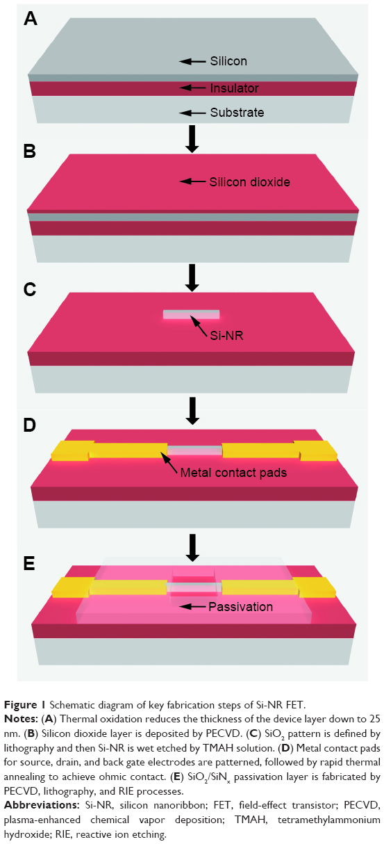 | Figure 1 Schematic diagram of key fabrication steps of Si-NR FET. |
Because of the etching selectivity of Si and SiO2 in the TMAH solution, only the area protected by the SiO2 layer remained in the solution; the rest was etched away. In this way, the device was patterned. After patterning, the SiO2 layer was removed by a buffered oxide etching (BOE) etchant.
A Ni/Au (20 nm/100 nm) bilayer was deposited and patterned on the wafer to define the contact area of the source, the drain, and the back gate. Ohmic contact was obtained by using rapid thermal annealing at 400°C (10°C/s; Figure 1D). SiO2/SiNx (200 nm/200 nm) was deposited as a passivation layer. The Si-NR detection window was opened by using reaction ion etching and BOE. The chamber of the RIE is a vacuum environment, with pressure always below 10–3 Pa and operating frequency between 10 and 100 MHz. (Figure 1E).
Figure 2 shows the 3D schematic diagram and sectional schematic of Si-NR. The size of a single device is 15×10 mm. There are five parallel Si-NRs on the device that can be observed in the detecting window, as shown in Figure 2A. One of the Si-NRs was characterized by scanning electron microscopy (SEM; Quanta 400 FEG, FEI Company, Hillsboro, OR, USA; Figure 2B and C). An SEM image of Si-NR device (length 30 μm) is shown in Figure 2B, and a corresponding zoomed-in image, showing the device with width 120 nm and length 25 nm, is shown in Figure 2C. On the device, a passivation layer was deposited by PECVD and patterned by lithography and the RIE process.
 | Figure 2 Morphology of the Si-NR FET device. (A) The 3D schematic diagram of the Si-NR FET device; (B) SEM image of the Si-NR FET device; and (C) SEM image of Si-NR. |
Surface functionalization of the Si-NR
Si-NRs should be covalently modified with monoclonal anti-CEA through the surface natural oxidation layer of Si-NRs for the purpose of CEA detection. The method using the linker of APTES bounded with Glu is one of the most well-known chemical covalent methods, wherein an aldehyde terminal is prepared for bonding with the detected protein.30,31 The same method was used in the study for surface functionalization. In this work, the surface of the Si-NR chip was cleaned by oxygen plasma (30 W and 50 sccm O2) for 5 min. After cleaning, because the sensor was inevitably exposed to air, an oxide layer was generated on the surface of the device.
The device was dipped into 2% (v/v) APTES anhydrous ethanol solution for 40 min. The amino groups were adhered onto the surface of Si-NR. After the modification, the unconjugated APTES and anhydrous ethanol on the chip surface were vapored by heat treatment at 120°C for 1 h. The bonded amino groups were connected with the aldehyde groups. The chip was dipped in 2.5% (v/v) Glu solution for 1 h. Finally, CEA monoclonal antibodies were covalently linked to the Si-NR surface by keeping the device at 4°C for 4 h. The surface functionalization process is schematically shown in Figure 3A.
 | Figure 3 Schematic illustration of Si-NR surface modification and microfluidic channel. (A) Si-NR surface modification with chemical covalent method; (B) SEM images of IgG-modified Si-NR; (C) BSA-modified Si-NR; (D) unmodified Si-NR with Au nanoparticles labeled anti-IgG conjugates; (E) schematic diagram of the Si-NR device integrated with PDMS microfluidic channel; and (F) optical image of the PDMS sealed device integrated with acrylic fastening fixture. |
To verify the functionalization result directly, a method using anti–IgG-labeled Au nanoparticles (10 nm) was used. Relevant results are shown in Figure 3B–D. Firstly, IgGs were modified on the surface of Si-NR by aldehyde groups, with BSA modified and unmodified devices as control samples. The sample modified by IgGs was immersed in the anti–IgG-labeled Au nanoparticles (10 nm) solution at 25°C for 8 h.
Anti–IgG-labeled Au nanoparticles can specifically combine with IgG on the surface of Si-NR. The immunological combination cannot be washed away by DI water. Therefore, Au nanoparticles remained on the surface of Si-NR all the time on the sample modified by IgGs. Figure 3B shows the modification process. In contrast, Au nanoparticles can rarely be observed on the surface of BSA modified and unmodified devices because anti–IgG-labeled Au nanoparticles are not combined with BSA. The SEM observation method is an effective way to evaluate the quality of the functionalization by calculating the number of nanoparticles combined on the Si-NR.23 The results shown in Figure 3B–D demonstrated this analysis. This is a direct evidence of the successful functionalization on the fabricated device.
After the functionalization process, a microfluidic channel was integrated on the top of the device. The CEA solution keeps flowing in the channel during the detection process. The microfluidics channel was fabricated with PDMS (Figure 3E).32 An acrylic fixture was utilized to increase the sealing between the microfluidic channel and biosensor (Figure 3F). During the measurement, a peristaltic pump was connected with the channel to transport CEA solutions through the sample vessels in a continuous flow.
Detection of CEA PBS buffer solutions
The relative change in current illustrates the sensing result for the detection of CEA solution containing 1 mg/mL BSA. When certain concentrations of CEA solution flowed in the microfluidic channel for 100 s, real-time detections were performed on the sample to derive the relationship between the Ids and time. All measurements were performed at room temperature (25°C±2°C).
Results and discussion
Electrical properties of the Si-NR FET
Figure 4 shows the influence on the sensor’s output properties when considering the variations of the sensor’s geometries. The width is 120±3 nm and the thickness is 25±2 nm. The error comes from multiple measurements and different samples. The variations have no significant influence on the electrical properties of the Si-NRs (P<0.01). To get the whole picture on the errors induced by the variations, the relative values were calculated by the formula of |ΔX|/ΔX, in which X refers to the actual measured values of the width, the height, and Ids, while ΔX denotes the corresponding variation. The calculated values |ΔX|/ΔX can be used to evaluate the relative variations and can be integrated in one figure, as shown in Figure 4.
 | Figure 4 The influence of the variation of the width and height of the Si-NRs on the Ids (Vgs =−15 V, Vds =5 V). |
The results demonstrate that the Si-NR FET shows an excellent uniformity and reproducibility. Moreover, the fabrication process of Si-NR is compatible with complementary metal oxide semiconductor (CMOS) technology,33–35 which can be used for mass production in future diagnostic applications.
The electrical properties of the Si-NR FET, including the output character (Id-Vds) and transport character (Id-Vgs), were measured on Agilent B1500A Semiconductor Device Analyzer (Agilent Technologies Inc., Santa Clara, CA, USA; Figure 5). The fabricated device shows a p-type property when a negative voltage or zero voltage is applied on the gate. When a positive voltage is applied on the gate, negative charge will be accumulated in the channel and n-type property will be shown. Therefore, the device shows typical ambipolar properties, which are controlled by the gate voltage. Typically, no voltage is applied during the characterization; therefore, the sensor shows p-type property during the subsequent characterization.
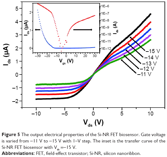 | Figure 5 The output electrical properties of the Si-NR FET biosensor. Gate voltage is varied from −11 V to −15 V with 1–V step. The inset is the transfer curve of the Si-NR FET biosensor with Vds =−15 V. |
This means the conductivity of the FET can be modulated either by positively charged species or negatively charged species such as proteins on the gate voltage. As depicted in the transport behavior, an on/off ratio of approximately 105–106 can be observed (Figure 5). The specific binding bond has charges and will influence the conductance of the channel in the transistor. If the bond is charged negatively, a positive charge will be induced in the channel. For the p-type transistor, this will increase the conductivity of the transistor.
Response behaviors of the CEA biosensor
Measurements on the output properties of the Si-NRs functionalized by monoclonal anti-CEA were conducted with different CEA concentrations, as shown in Figure 6. Vgs =−5 V was applied on the back gate in the measurement, which can increase homogeneous distribution of the electric field. The results in Figure 6 show that different CEA solutions, with concentrations of 1, 10, and 100 ng/mL, separately, have an obvious influence on the output properties. For example, the output result corresponding to 1 ng/mL concentrations was saturated at 0.2 μA when the applied voltage was >6 V. However, the output results of two other samples with 10 and 100 ng/mL kept increasing constantly with current much higher than the result of 1 ng/mL. Since all other parameters are the same, except for different CEA concentrations, the results in Figure 6 demonstrate that the device is very sensitive to the CEA concentration. To the authors’ knowledge, the sensitivity coincides with results reported by other groups.21 A control sample was also used in the experiment, with 0.01× PBS flowing during measurement. When the 0.01× PBS buffer without CEA flows through the microfluidic channel, the current does not increase. This demonstrates that the output of the sensor is specifically sensitive to the CEA.
 | Figure 6 Output curves of functionalized Si-NRs biosensor with different concentrations of CEA. The Si-NR biosensor is functionalized by monoclonal anti-CEA, and concentrations 1, 10, and 100 ng/mL are sequentially delivered in the channel. Output results of a sample treated with 0.01× PBS are also included as control sample. |
The Ids saturation current kept increasing with the increment of the concentration of CEA solution, as shown in Figure 7. Figure 7A shows the current corresponding to different concentrations of CEA. The concentrations of CEA solutions are 10, 100, 1, 10, and 100 ng/mL, separately. It shows clearly that the currents are increased monologically with increasing CEA concentration (Figure 7A). In Figure 7, the regions of Ids near to zero refer to the interval periods, in which different concentrations of CEA solutions were changed from the previous one to the next one. To rid the influence of the previous flow solution, air bubbles were used to clean the channel. This is the main reason for the current to approach zero during the interval period.
 | Figure 7 Real-time detection of various concentrations of CEA protein on Si-NR FET biosensor. (A) Time–current curves of different concentrations of CEA (red curve) and BSA (black curve) 0.01× PBS solutions flowed through the microfluidic channel. The numbers under the curve correspond to times when solutions of: 1) 0.05% BSA PBS solution, 2) 10 pg/mL CEA, 3) 100 pg/mL CEA, 4) 1 ng/mL CEA, 5) 10 ng/mL, and 6) 100 ng/mL are flowing in the microfluidic channel. In Figure 7, the regions of Ids near to zero refer to the interval periods, in which different concentrations of CEA solutions were changed from the previous one to the next one. To rid the influence of previous flowing solution, air bubbles were used to clean the channel. This is the main reason for the current approaching zero during the interval period. (B) The logarithm of CEA solutions concentrations versus the current change ratio. Error bars (P<0.01). |
To rid other unexpected aspects that may influence the time–Ids relationship, BSA solution was also allowed to flow through the sample for the same duration. As shown in Figure 7A, there is no influence of BSA on Ids. Therefore, this confirms that the main reason for the Ids change comes from the difference of CEA concentrations.
To gain a better understanding of the relationship between the currents and CEA concentrations, a logarithmic axis is used (Figure 7B). The calibration curve can be fitted as Ids =122.34+22.40 ln (CCEA). The detection resolution is measured to be 10 pg/mL.
To obtain a clear comparison of the whole picture, published relevant data from several groups and our results are summarized in Table 1. Quantitative detection of CEA concentration can be achieved when normalizing the obtained values to different CEA concentrations. This approach offers good specificity and sensitivity, with a detection sensitivity of 10 pg/mL. The proposed Si-NR FET biosensor possesses similar detection sensitivity with previous reports from other groups.36–41 The detections are very promising in terms of the simultaneous determination of multiple tumor markers in one assay of serum.
 | Table 1 Comparison of the performance of sensors in detection of CEA |
For results from other groups, the sensitivity of the measurement was related to the size of nanosensors. The main reason is based on the fact that SiNW biosensors are not uniform in size. The biosensor would become more sensitive with a reduced-size SiNW. However, the repeatability of the biosensors may not be ideal. To investigate the repeatability of the biosensor, we measured 60 devices and confirmed that the fabricated devices show ideal repeatability.
To obtain homogeneous distribution of the electric field across the entire thickness, the thickness of Si-NR should be scaled down. In this way, repeatable nanoarrays biosensor with high sensitivity can be achieved. However, the aggressively scaled dimensions of the Si-NRs are not necessary in this approach.
Conclusion
A label-free, real-time, and sensitive Si-NR FET biosensor that represents the powerful capability of biomolecule detection is reported in this paper. The Si-NR FET biosensor is fabricated by a top–down approach, which is comparable to the massive fabrication CMOS technology. The electrical properties of the devices are repeatable, which could be a benefit in the quantitative detection of the target molecule. The biosensor is verified by using different concentrations of CEA solutions, showing that the device has potential valuable applications in diagnostics and life sciences.
Acknowledgments
This work was supported by grants from the National Natural Science Foundation of China (no 81371683/H1819), Clinical Medicine Project of Jiangsu Province (no BL2014023), and Young Talents Hausen Fund of Lianyungang Clinical College in China (no QN160304).
Disclosure
The authors report no conflicts of interest in this work.
References
Byström P, Berglund Å, Nygren P, et al. Evaluation of predictive markers for patients with advanced colorectal cancer. Acta Oncol. 2012;51(7):849–859. | ||
Kim JY, Kim NK, Sohn SK, et al. Prognostic value of postoperative CEA clearance in rectal cancer patients with high preoperative CEA levels. Ann Surg Oncol. 2009;16(10):2771–2778. | ||
Spencer SKM, Pommier AJC, Morgan SR, et al. Prognostic/predictive value of 207 serum factors in colorectal cancer treated with cediranib and/or chemotherapy. Br J Cancer. 2013;109(11):2765–2773. | ||
Schneider J, Velcovsky HG, Morr H, Katz N, Neu K, Eigenbrodt E. Comparison of the tumor markers tumor M2-PK, CEA, CYFRA 21-1, NSE and SCC in the diagnosis of lung cancer. Anticancer Res. 2000;20(6D):5053–5058. | ||
Foa P, Fornier M, Miceli R, et al. Tumour markers CEA, NSE, SCC, TPA and CYFRA 21.1 in resectable non-small cell lung cancer. Anticancer Res. 1999;19(4C):3613–3618. | ||
Diez M, Pollan M, Maestro ML, et al. Concordance between serum and cytosolic levels of CEA, CA125 and SCC antigens in patients with non-small cell lung cancer. Anticancer Res. 1995;15(6B):2811–2817. | ||
Jafarpour-Sadegh F, Montazeri V, Adili A, et al. Effects of fresh yellow onion consumption on CEA, CA125 and hepatic enzymes in breast cancer patients: a double-blind randomized controlled clinical trial. Asian Pac J Cancer Prev. 2015;16(17):7517–7522. | ||
Park BJ, Cha MK, Kim IH. Thioredoxin 1 as a serum marker for breast cancer and its use in combination with CEA or CA15-3 for improving the sensitivity of breast cancer diagnoses. BMC Res Notes. 2014;7:7. | ||
Mathew J, Prinsloo P, Agrawal A, et al. Pilot randomised study of early intervention based on tumour markers in the follow-up of patients with primary breast cancer. Breast. 2014;23(5):567–572. | ||
Premkumar VG, Yuvaraj S, Vijayasarathy K, Gangadaran SG, Sachdanandam P. Effect of coenzyme Q10, riboflavin and niacin on serum CEA and CA 15-3 levels in breast cancer patients undergoing tamoxifen therapy. Biol Pharm Bull. 2007;30(2):367–370. | ||
Kloudová K, Hromádková H, Partlová S, et al. Expression of tumor antigens on primary ovarian cancer cells compared to established ovarian cancer cell lines. Oncotarget. 2016;7(29):46120–46126. | ||
Bian J, Li B, Kou XJ, Wang XN, Sun XX, Ming L. Clinical applicability of multi-tumor marker protein chips for diagnosing ovarian cancer. Asian Pac J Cancer Prev. 2014;15(19):8409–8411. | ||
Kondalsamy-Chennakesavan S, Hackethal A, Bowtell D; Australian Ovarian Cancer Study Group, Obermair A. Differentiating stage 1 epithelial ovarian cancer from benign ovarian tumours using a combination of tumour markers HE4, CA125, and CEA and patient’s age. Gynecol Oncol. 2013;129(3):467–471. | ||
Hefta LJ, Neumaier M, Shively JE. Kinetic and affinity constants of epitope specific anti-carcinoembryonic antigen (CEA) monoclonal antibodies for CEA and engineered CEA domain constructs. Immunotechnology. 1998;4(1):49–57. | ||
Huyghe J. CEA radioimmunoassay. Clinical applications in colorectal cancer. Acta Chir Belg. 1983;83(2):77–88. | ||
Lin J, Chu P, Wei Z. A new dual immunoassay for tumor markers based on chemiluminescence signal amplification by magnetic mesoporous silica and enzyme modified gold nanoparticles. Anal Sci. 2012;28(1):21–25. | ||
Pei X, Chen B, Li L, Gao F, Jiang Z. Multiplex tumor marker detection with new chemiluminescent immunoassay based on silica colloidal crystal beads. Analyst. 2010;135(1):177–181. | ||
Matsushita H, Xu J, Kuroki M, et al. Establishment and evaluation of a new chemiluminescent enzyme immunoassay for carcinoembryonic antigen adapted to the fully automated ACCESS system. Eur J Clin Chem Clin Biochem. 1996;34(10):829–835. | ||
Cui Y, Wei Q, Park H, Lieber CM. Nanowire nanosensors for highly sensitive and selective detection of biological and chemical species. Science. 2001;293(5533):1289–1292. | ||
Patolsky F, Zheng G, Lieber CM. Nanowire sensors for medicine and the life sciences. Nanomedicine (Lond). 2006;1(1):51–65. | ||
M Nuzaihan MN, Hashim U, Md Arshad MK, et al. Top-down nanofabrication and characterization of 20 nm silicon nanowires for biosensing applications. PLoS One. 2016;11(3):e0152318. | ||
Shen MY, Li BR, Li YK. Silicon nanowire field-effect-transistor based biosensors: from sensitive to ultra-sensitive. Biosens Bioelectron. 2014;60:101–111. | ||
Presnova G, Presnov D, Krupenin V, et al. Biosensor based on a silicon nanowire field-effect transistor functionalized by gold nanoparticles for the highly sensitive determination of prostate specific antigen. Biosens Bioelectron. 2017;88:283–289. | ||
Zhang A, Lieber CM. Nano-bioelectronics. Chem Rev. 2016;116(1):215–257. | ||
Li J, He G, Ueno H, et al. Direct real-time detection of single proteins using silicon nanowire-based electrical circuits. Nanoscale. 2016;8(36):16172–16176. | ||
Lin MC, Chu CJ, Tsai LC, et al. Control and detection of organosilane polarization on nanowire field-effect transistors. Nano Lett. 2007;7(12):3656–3661. | ||
Smaali K, Guérin D, Passi V, et al. Physical study by surface characterizations of sarin sensor on the basis of chemically functionalized silicon nanoribbon field effect transistor. J Phys Chem C. 2016;120(20):11180–11191. | ||
Chen Y, Ren R, Pu H, Chang J, Mao S, Chen J. Field-effect transistor biosensors with two-dimensional black phosphorus nanosheets. Biosens Bioelectron. 2016;89(Pt 1):505–510. | ||
Schwierz F, Pezoldt J, Granzner R. Two-dimensional materials and their prospects in transistor electronics. Nanoscale. 2015;7(18):8261–8283. | ||
Kong T, Su R, Zhang B, Zhang Q, Cheng G. CMOS-compatible, label-free silicon-nanowire biosensors to detect cardiac troponin I for acute myocardial infarction diagnosis. Biosens Bioelectron. 2012;34(1):267–272. | ||
Sharma RK, Sharma S. Silica nanosphere-supported palladium(II) furfural complex as a highly efficient and recyclable catalyst for oxidative amination of aldehydes. Dalton Trans. 2014;43(3):1292–1304. | ||
Patolsky F, Zheng G, Lieber CM. Fabrication of silicon nanowire devices for ultrasensitive, label-free, real-time detection of biological and chemical species. Nat Protoc. 2006;1(4):1711–1724. | ||
Za’bah NF, Kwa KSK, Bowen L, Mendis B, O’Neill A. Top-down fabrication of single crystal silicon nanowire using optical lithography. J Appl Phys. 2012;112(2):024309. | ||
Vu XT, Ghoshmoulick R, Eschermann JF, Stockmann R, Offenhäusser A, Ingebrandt S. Fabrication and application of silicon nanowire transistor arrays for biomolecular detection. Sens Actuators B Chem. 2010;144(2):354–360. | ||
Rius G, Llobet J, Borrisé X, Pérez-Murano F. Fabrication of nanomechanical devices integrated in CMOS circuits by ion beam exposure of silicon. AIP Conf Proc. 2011;1336(1):239–242. | ||
Cao X, Wang N, Jia S, Guo L, Li K. Bimetallic AuPt nanochains: synthesis and their application in electrochemical immunosensor for the detection of carcinoembryonic antigen. Biosens Bioelectron. 2013;39(1):226–230. | ||
Zhao D, Wang Y, Nie G. Electrochemical immunosensor for the carcinoembryonic antigen based on a nanocomposite consisting of reduced graphene oxide, gold nanoparticles and poly(indole-6-carboxylic acid). Microchimica Acta. 2016;183(11):2925–2932. | ||
Hu M, Yan J, He Y, et al. Ultrasensitive, multiplexed detection of cancer biomarkers directly in serum by using a quantum dot-based microfluidic protein chip. ACS Nano. 2010;4(1):488–494. | ||
Pang X, Li J, Zhao Y, et al. Label-free electrochemiluminescent immunosensor for detection of carcinoembryonic antigen based on nanocomposites of GO/MWCNTs-COOH/Au@CeO2. ACS Appl Mater Interfaces. 2015;7(34):19260–19267. | ||
Chen L, Zeng X, Si P, et al. Gold nanoparticle-graphite-like C3N4 nanosheet nanohybrids used for electrochemiluminescent immunosensor. Anal Chem. 2014;86(9):4188–4195. | ||
Zhou L, Mao H, Wu C, et al. Label-free graphene biosensor targeting cancer molecules based on non-covalent modification. Biosens Bioelectron. 2017;87:701–707. |
 © 2017 The Author(s). This work is published and licensed by Dove Medical Press Limited. The
full terms of this license are available at https://www.dovepress.com/terms
and incorporate the Creative Commons Attribution
- Non Commercial (unported, 3.0) License.
By accessing the work you hereby accept the Terms. Non-commercial uses of the work are permitted
without any further permission from Dove Medical Press Limited, provided the work is properly
attributed. For permission for commercial use of this work, please see paragraphs 4.2 and 5 of our Terms.
© 2017 The Author(s). This work is published and licensed by Dove Medical Press Limited. The
full terms of this license are available at https://www.dovepress.com/terms
and incorporate the Creative Commons Attribution
- Non Commercial (unported, 3.0) License.
By accessing the work you hereby accept the Terms. Non-commercial uses of the work are permitted
without any further permission from Dove Medical Press Limited, provided the work is properly
attributed. For permission for commercial use of this work, please see paragraphs 4.2 and 5 of our Terms.