Back to Journals » International Journal of Nanomedicine » Volume 15
Implementation of PPI with Nano Amorphous Oxide Semiconductor Devices for Medical Applications
Authors Dai M ![]() , Wu Z, Qi S, Huo C, Zhang Q, Zhang X, Webster TJ
, Wu Z, Qi S, Huo C, Zhang Q, Zhang X, Webster TJ ![]() , Zhang H
, Zhang H
Received 7 March 2019
Accepted for publication 28 August 2019
Published 17 March 2020 Volume 2020:15 Pages 1863—1870
DOI https://doi.org/10.2147/IJN.S207852
Checked for plagiarism Yes
Review by Single anonymous peer review
Peer reviewer comments 2
Editor who approved publication: Prof. Dr. Anderson Oliveira Lobo
This paper has been retracted.
Mingzhi Dai, 1 Zhendong Wu, 1 Shaocheng Qi, 1 Changhe Huo, 1 Qiang Zhang, 1 Xingye Zhang, 1 Thomas J Webster, 2 Hengbo Zhang 1
1Ningbo Institute of Materials Technology and Engineering, Chinese Academy of Sciences, Ningbo 315201, People’s Republic of China; 2Department of Chemical Engineering, Northeastern University, Boston, MA 02115, USA
Correspondence: Mingzhi Dai Email [email protected]
Background: Electronic devices which mimic the functionality of biological synapses are a large step to replicate the human brain for neuromorphic computing and for numerous medical research investigations. One of the representative synaptic behaviors is paired-pulse facilitation (PPF). It has been widely investigated because it is regarded to be related to biological memory. However, plasticity behavior is only part of the human brain memory behavior.
Methods: Here, we present a phenomenon which is opposite to PPF, i.e., paired-pulse inhibition (PPI), in nano oxide devices for the first time. The research here suggests that rather than being enhanced, the phenomena of memory loss would also be possessed by such electronic devices. The device physics mechanism behind memory loss behavior was investigated. This mechanism is sustained by historical memory and degradation manufactured by device trauma to regulate characteristically stimulated origins of artificial transmission behaviors.
Results: Under the trauma of a memory device, both the signal amplitude and signal time stimulated by a pulse are lower than the first signal stimulated by a previous pulse in the PPF, representing a new scenario in the struggle for memory. In this way, more typical human brain behaviors could be simulated, including the effect of age on latency and error generation, cerebellar infarct, trauma and memory loss pharmacological actions (such as those caused by hyoscines and nitrazepam).
Conclusion: Thus, this study developed a new approach for implementing the manner in which the brain works in semiconductor devices for improving medical research.
Keywords: artificial bio synapses, ion dynamics, PPI, paired-pulse pulse inhibition, memory loss
Corrigendum for this paper has been published
Introduction
Synaptic behaviors are important to investigate and implement because neuromorphic computing has been proposed as a new computing paradigm to analyze complex information like that from the brain.1–3 This has promulgated the development of “next-generation” nanodevices that have unique functions and characteristics.4 In recent years, many kinds of electronic devices have been used successfully to produce artificial synapses. For example, Kim et al reported that a three-terminal synaptic transistor based on carbon nanotubes can provide reliable synaptic functions that encodes relative timing and regulates weight change.5 Zou et al also reported the fabrication of tin oxide (SnO2) nanowire synaptic transistors using polymer–electrolyte gating. The fabricated devices not only exhibited excellent performance but also can mimic important synaptic behavior.6 Esqueda et al also presented aligned carbon nanotube (CNT) synaptic transistors for large-scale neuromorphic computing systems. The synaptic behavior of these devices was achieved via charge-trapping effects, commonly observed in carbon-based nanoelectronics.7 Therefore, important artificial synapse devices are needed to realize the synaptic behaviors in neuromorphic systems. Representative synaptic behaviors include information memory and processing. Such synaptic behaviors are initiated by the dynamics of Ca2+ ion transport influx among synapses.4,5 When a stimulation such as an action potential drives an influx of ions to reach a synapse, the neurotransmitters are stimulated and released. The transfer mechanism of ion dynamics is analogous to that of Ca2+ dynamics in a biological synapse. In this way, the use of ionic semiconductor channels in electronic devices could be a useful way to emulate the biological synapses. The devices include both resistors, capacitors, transistors and circuits. Here, nanoscale inorganic transistors are employed for neurocomputing and for improving medical research.6–14
Amorphous oxide semiconductor (AOS) devices have attracted much attention in recent years. One of the representative materials is In-Ga-Zn-O (IGZO). IGZO has been one of the most popular AOS materials since it was published in 2004. They have some attractive properties, including transparency, flexibility, and relatively low-cost fabrication mainly attributed to the low temperature processing at no higher than 200°C.15–19 Most of AOS are n-type materials. This is because p-type AOS materials have carrier mobilities much lower than n-type AOS materials. What is more, p-type AOS materials are different from n-type materials and are regarded to be much more difficult to obtain. AOS has been regarded as a potential candidate to use in displays and portable sensors.
Here, this paper shows some typical synaptic characteristics, based on an IGZO thin-film transistor (TFT) structure. Some representative synaptic behaviors are investigated. For instance, the artificial synapse that emulates a “plasticity” of a response is required for the development of neuromorphic computing systems. One typical transmission behavior is the excitatory postsynaptic current (EPSC).7–12 An important plasticity behavior is paired-pulse facilitation (PPF).20–23 In comparison, the synaptic behaviors mimicked by the three terminal transistors are easier to control than the two terminal devices.24,25 This paper suggests the feasibility of using semiconductor devices to study memory loss dynamics, which helps in the development of the biocompatible and biodegradable artificial synapse devices for medical applications.
Materials and Methods
Fabrication of Artificial Synapse Devices. The artificial device of this study had the IGZO TFT bottom gate structure (Figure 1B). A SiO2/Si substrate was purchased and used as the bottom gate and dielectric layer (100 nm thick). The IGZO channel was then deposited using radio-frequency (RF) magnetron sputtering. The Ar:O2 was in the range from about 5:3 to 5:0. The deposition time was about 5 mins. The vacuum was ~6 × Torr. Afterwards, about a 25 nm-thick IGZO was deposited and the patterns with the specifically designed channel lengths and widths were defined by lithography and wet etching. The width and length were in micrometers, which could be scaled down by using more advanced lithography techniques such as e-beam lithography. Subsequently, the electrode patterns were defined by the masks made by lithography. The top electrodes were formed by thermal evaporation through a shadow mask formed by a photoresist. The 10 nm Ti adhesion layer was then deposited using an e-beam evaporator in a vacuum of ~4 ×10⁻⁶ Torr. A 10 nm Au top electrode layer was then deposited after Ti deposition in the same e-beam evaporator chamber to act as the conduction layer and protection layer for Ti. The photoresistor layer which prevents metal electrode deposition was consequently removed by ultrasonication and cleaned in acetone, ethanol, and distilled water for 20 min each. The bottom gate TFT structure was annealed at 475 K for 2 h. The length and width of the electrode lines were 30–100μm and 100μm, respectively. The length and width of the electrode in a square were 120–150μm.
Characterization. The measurement of the electrical properties and curves were all performed at room temperature and atmospheric pressure. The current−voltage (I−V) curve including transfer curves (IDS vs VGS) and the time dependence of the discharge current and diffusion potential were measured by using a semiconductor parameter analyzer (4200-SCS, Keithley). The current responses under the pulses were obtained by using the pulse mode of a Keithley 4200. During the electrical measurements, the Ti/Au source electrode was electrically grounded, and an external bias was applied to the Si bottom gate electrode. A top view of IGZO TFT was captured using high-resolution field-emission scanning electron microscopy (FE-SEM, JSM-7401F,JEOL) at a 5 kV acceleration voltage (Figure 1C).
Results and Discussion
Figure 1 shows the IGZO sample structure. Figure 1A is a representative synapse. Figure 1B shows a typical TFT bottom gate structure. Here, the bottom gate TFT was used and fabricated which is more convenient in the lab. However, the top gate TFT could also be used to realize similar synaptic behaviors.8,9,16-18 The IGZO transistor samples were fabricated using the following steps which are very common for lab study. The fabrication was based on a wafer with n-type Si as the bottom gate layer and a 100-nm thick SiO2 as an insulating layer on top. This could be purchased from the fabrication company. The IGZO channel layer and electrodes were deposited in the lab by us. The IGZO semiconductor layer was then deposited by radio-frequency (RF) magnetron sputtering. The thickness and quality of the IGZO film could be controlled and adjusted by deposition time, power and gas flow ratio. Here, Ar: O2 was around 3:0. The 25–50 nm-thick IGZO semiconductor channel was then patterned by lithography, with the width/length ranging from 3 to 400 μm. The electrodes for the source and drain were then deposited and patterned. These electrodes were deposited by electron beam evaporation. The thickness and quality of the films could be controlled also by the deposition time and speed. Here, the electrodes were Ti/Au with 80 nm/14 nm thickness, respectively.
In this artificial synapse, the Ti/Au electrodes are used as the drain and source which are connected with the IGZO channel, as shown in Figure 1B. The gate voltage is defined as VGS and the drain voltage is VDS. The source voltage is always grounded to be 0 V. The channel current is the drain current measured from the drain and defined as IDS. The IGZO channel has metal ions which could provide mobile carriers, including electrons and holes, to transport from the source to the drain (or vice versa), and to inject into the insolating layer SiO2, when given proper VGS and VDS. The transport of the mobile ions is similar to the way ions move in the synapses. Therefore, we could use the IGZO TFT to mimic the representative artificial synaptic transmission behaviors, including EPSC and PPF.13,14,21,22 The procedure of mimicking is as follows: A pulse with an amplitude VO is applied as VGS on the bottom gate terminal. As Figure 1B shows, when the pulse is applied on the gate, IDS could be stimulated, measured and demonstrated as a representative transmission behavior, EPSC. Figure 1C shows the SEM image of the sample TFT top view with an IGZO channel. Figure 1D shows the cross-section image of the TFT structure, with different layers from the bottom gate, dielectric layer, and channel layer to the metal layers.
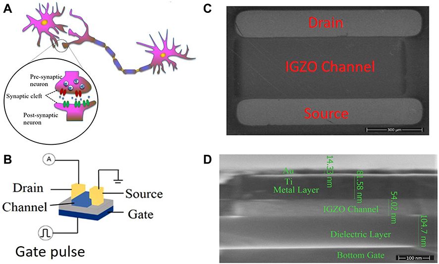 |
Figure 1 Schematic of the IGZO-based artificial bio synapses, i.e., IGZO TFT. (A) The typical structure of synapses, including the synaptic cleft: pre- and postsynaptic neuron parts. (B) A IGZO TFT device bottom gate structure and the proposed measurement of representative synaptic transmission behavior in IGZO TFT. (Voltage is applied to the bottom gate, and the drain current is the bionic neural signal). (C) SEM top image of IGZO TFTs with an IGZO channel between the source and the drain top electrodes (scale bar=300μm). (D) SEM image of IGZO TFTs layers cross section (scale bar = 100 nm). |
The measured I-T is shown in Figure 2. When a DC voltage sweeps from 0V to 30V and decreases to 5V after holding 5s. (0 V → 30 V → 5 V), the status of IGZO TFT is from turn-off to turn-on, i.e., with IDS reaching a maximum current Io in a transient way and decreasing slowly back to the off state. In general, under an electric field, the active metal ion functional groups and insulating layer could have carrier charging interactions. The channel could then move from the semiconductor to conductive layer. When the pulse is applied, the channel current increases abruptly to the compliance current (CC) level at the Vo level, which means the channel changes from insulating to conducting. When the pulse is released, the channel current decreases back, which corresponds to the channel changing from conducting back to insulating. The measured curve in Figure 2 fits a simple exponential function which is similar to synaptic transmission behavior, such as EPSC.13,14,26 This simple exponential function is described as:
(1)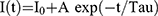
where Tau and A are the relaxation time and the prefactor, I0 is the current level when the IGZO TFT voltage is at 5V steady state, and I(t) is the current level at the time t.
 |
Figure 2 Typical and representative electrical transmission behavior of the IGZO-based artificial bio synapses. (A) Relaxation characteristic of an artificial synapse. (B) Current level measurement and fitting of the relaxation of an artificial synapse based on the IGZO TFTs. |
This transmission behavior is due to the charging and discharging of the mobile carriers stimulated by the gate pulse. The process is illustrated in Figure 3. The pulse consists of an amplitude of Vo and a base voltage of 0 V. Before the Vo pulse is applied, at stage ①, the carriers are not attracted to the interface between the IGZO channel and the insulating layer SiO2. Afterwards, a pulse with an amplitude of Vo is applied, it could bring a change in the IGZO TFT which includes functional groups such as Zn-O, In-O, and Ga-O. These functional groups could interact with metal ions and persist in the channel and in metal ions and oxide carriers. At stage ② when VGS increases from 0 to Vo, the mobile carriers in the channel are activated and attracted to the interface between the IGZO and the SiO2 layer. The mobile carriers could continue to stay within the interface of IGZO-SiO2, even further injecting into the defects and get trapped, during stage ③ when VGS is kept at Vo. At stage ④ when the pulse with an amplitude Vo is released and VGS decreases from Vo to 0 V, the mobile carriers which are attracted to the interface channel are driven back into the source and the drain. At stage ⑤ when VGS is returned to 0 V, the trapped charges are injected in the defects which respond more slowly than the mobile carriers in the channel and are driven back to the source and the drain.
 |
Figure 3 Overview of a voltage pulse profile and the corresponding discharge current in the TFTs with the IGZO channel in red (trapped electrons, mobile carriers trapped by interface between the IGZO and the SiO2 layer or defects). The number for the sub-images on the right correspond to each respective numbered region in the schematic on the left. |
A previous study mainly focussed on the materials, device structure, and pulse number impact on artificial synaptic behaviors. Here, we focus on the impact on pulse amplitude on the paired-pulse regulations. In this way, oxide devices could be used to implement the functionalities of PPF and PPI.21–23 Therefore, the oxide electronic devices have the potential to mimic biological synapse characteristics, not only in information processing (such as writing and erasing data), but also in both representative synaptic behaviors including memorizing and processing information and memory loss ways.17,18
As shown in Figure 4, the PPF could be obtained by applying a VGS pulse with Vo = 30 V which lasts for 5ms.23,24 The CC corresponding to the former pulse is smaller than that for the latter pulse. This shows the CC have an accumulation effect after each pulse. This is reasonable, because the trapped charges are moving slowly so that some might remain in the defects during stage ⑤, and increase the CC in the next pulse. This suggests that when VGS is no higher than 30 V, the PPF could be obtained and the related mechanism dominant. The mechanism could be mainly attributed to the reason that the mobile charges trapped in the defects are not released completely during stage ⑤. The CC for the second pulse could include the unreleased charges for the first pulse and increase. This means the time space between the two pulses, i e, Δt is not large enough.
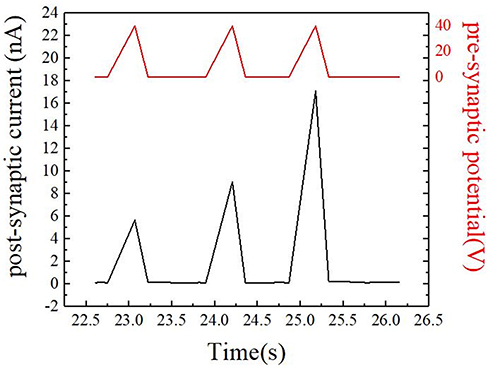 |
Figure 4 Experimental demonstration of paired-pulse facilitation (PPF) through the discharge current stimulated by voltage pulse on the IGZO. |
When pulse intervals are short, because of plasticity behavior, synaptic will produce a PPI effect. In order to observe a significant PPF effect, we increased the pulse intervals from 0.75s to 3s, so that the PPI effect could be weakened. As shown in Figure 5, PPI could be implemented by applying a VGS pulse with Vo = 40 V for 5ms. The first stimulated CC is a maximum. This means that the mobile charges stimulated by the former pulse do not remain to increase the CC in the next pulse.20–23 This has two possible reasons. 1. The mobile charges have released completely during stage ⑤. 2. The mobile charges trapped in the defects would lead to a decrease of CC. As for reason 1, because the mobile charges during the 30 V pulse are not released between the pulses, it is unlikely the charges are released during a pulse of 40 V. The 40 V pulse is higher than 30 V and should attract more charges and would release completely during the same Δt in Figures 4 and 5.
 |
Figure 5 Experimental demonstration of paired-pulse inhibition (PPI) through the discharge current stimulated by voltage pulse on the IGZO TFT. |
To investigate the effect of voltage stress on the device insulators, different voltage conditions were applied in order to obtain a transfer curve and the loops are compared.14–16 As can be seen in Figure 6, a large hysteresis window of transfer curves should be attributed to trapped carriers. When VGS increases up to 30 V, as shown in Figure 6A, the hysteresis window is small. This means there were no defects during the 30 V VGS stress. When VGS increased up to 40 V, as shown in Figure 6B, the hysteresis window was significant. This suggests that 40V VGS, unlike 30 V VGS, had an impact on device film quality and performance. The hysteresis direction is clock-likewise and it suggests electron injection into the insulator. This reason is feasible because when electrons are injected into the TFT insulator by 40 V VGS, the actual VGS effect applied on the channel could be reduced so that IDS and thus CC is reduced at the same VGS. Because, when enough VGS is applied on the gate and a proper VDS applied on drain, a strong electric field would be generated near the drain. Electrons get enough energy in such a field on the drain edge could be injected into the gate oxide and cause damages at the interface and even within the oxide, which is called a hot carrier injection (HCI). Some TFT parameters would decrease caused by HCI, such as the threshold voltage, transconductance, channel mobility, and the drain current IDS.27–29 Therefore, the transfer curve of the sample under 40 V showed a decreased IDS when VGS is returned from 40 V to 0 V, which is consistent with the decrease of the current amplitude as shown in Figure 5. This clock-likewise hysteresis and thus the electron injection mechanism are consistent with the observations that CC decreases at pulses of 40 V VGS.
 |
Figure 6 Hysteresis of transfer curve for the IGZO TFT. (A) Transfer curve for the IGZO TFT, during the 30 V VGS stress. (B) Transfer curve for the IGZO TFT, during the 40V VGS stress. |
When a series of voltage pulses at a frequency of 667 Hz and an amplitude of 30 V are applied to the IGZO TFT, a short-term plasticity (STP) can be observed as shown in Figure 7. In the first six pulses, the CC continues to increase. The reason explained here is similar to the explanation of PPF, since the trapped charges are moving slowly, there may be some residual in the defect during stage ⑤ and CC, therefore, rises in the next pulse. When a pair of pulses continues to be applied, CC tends to stabilize. This may be due to the trapped charges injected into the defects reaching saturation. Trapped charges spontaneously returned to their original position and led to STP after the weak stimuli (10 pulses) ceased.
 |
Figure 7 Verification of short-term plasticity (STP) of the IGZO-based artificial bio synapses under a 10 pulses mode. |
Conclusions
In summary, PPI was observed for the first time on nano oxide electronic transistors. Representative artificial synaptic behaviors, such as synaptic transmission, PPF and PPI were processed and mimicked here. These functions were realized by the metal dynamics in the nano oxide artificial synapse. When an electrical stimulus was applied, the artificial bio synapse had a temporary increase and then spontaneous decay of conductance along time. The increase in conductance could be amplified or reduced by applying successive stimuli at short intervals. Repeated stimuli made the transition have a residual current for the next round of CC, or could have electrons injected to decrease the next round of CC due to the large amplitude and Vo impact on the device insulator. This research could, thus, help improve neuromorphic electronics for neurocomputing based on biocompatible artificial synapses as well as the development of medical research.
Acknowledgments
M. Dai was supported by the National Natural Science Foundation of China (Grant Nos 61106090, 61574147, 61274132), Zhejiang Provincial Natural Science Foundation for Distinguished Young Scholar (No. R17F040007), Ningbo Municipal Natural Science Foundation (No. 2014A610011), the Ningbo Natural Science Foundation of China (Grant Nos 2015A610034, 2011A610110, No. 2014B82004, Y10814VA0, 2016A610280), the State Key Basic Research Program of China (2013CB922300), Youth Innovation Promotion Association, the Chinese Academy of Sciences and the Royal Academy of Engineering, UK.
Disclosure
The authors report no conflicts of interest in this work.
References
1. Brunel D, Anghel C, Kim DY, et al. Integrating multiple resistive memory devices on a single carbon nanotube. Adv Funct Mater. 2013;23(45):5631–5637.
2. Xiao X, Beechem TE, Brumbach MT, et al. Lithographically defined three-dimensional graphene structures. ACS Nano. 2012;6(4):3573–3579. doi:10.1021/nn300655c
3. Dai X, Nguyen BM, Hwang Y, Soci C, Dayeh SA. Novel heterogeneous integration technology of III–V layers and InGaAs FinFETs to silicon. Adv Funct Mater. 2014;24(28):4420–4426. doi:10.1002/adfm.201400105
4. Vogel E. Technology and metrology of new electronic materials and devices. Nat Nanotechnol. 2007;2(1):25–32. doi:10.1038/nnano.2006.142
5. Kim S, Yoon J, Kim H-D, Choi S-J. Carbon nanotube synaptic transistor network for pattern recognition. ACS Appl Mater Interfaces. 2015;7(45):25479–25486. doi:10.1021/acsami.5b08541
6. Zou C, Sun J, Gou G, et al. Polymer–electrolyte-gated nanowire synaptic transistors for neuromorphic applications. Appl Phys A. 2017;123(9):597. doi:10.1007/s00339-017-1218-5
7. Esqueda IS, Yan X, Rutherglen C, et al. Aligned carbon nanotube synaptic transistors for large-scale neuromorphic computing. ACS Nano. 2018;12(7):7352–7361. doi:10.1021/acsnano.8b03831
8. Arnold AJ, Razavieh A, Nasr JR, Schulman DS, Eichfeld CM, Das S. Mimicking neurotransmitter release in chemical synapses via hysteresis engineering in MoS2 transistors. ACS Nano. 2017;11(3):3110–3118. doi:10.1021/acsnano.7b00113
9. Lamprecht R, Ledoux J. Structural plasticity and memory. Nat Rev Neurosci. 2004;5(1):45–54. doi:10.1038/nrn1301
10. Kim K, Chen CL, Truong Q, Shen AM, Chen Y. A carbon nanotube synapse with dynamic logic and learning. Advan Mater. 2013;25(12):1692. doi:10.1002/adma.201370080
11. Dai M, Wang W, Wang P, Iqbal MZ, Annabi N, Amin N. Realization of tunable artificial synapse and memory based on amorphous oxide semiconductor transistor. Sci Rep. 2017;7(1):10997. doi:10.1038/s41598-017-04641-5
12. Lai Q, Zhang L, Li Z, Stickle WF, Williams RS, Chen Y. Ionic/electronic hybrid materials integrated in a synaptic transistor with signal processing and learning functions. Advan Mater. 2010;22(22):2448–2453. doi:10.1002/adma.v22:22
13. Song J, Ampatzis K, Björnfors ER, El MA. Motor neurons control locomotor circuit function retrogradely via gap junctions. Nature. 2016;529(7586):399–402. doi:10.1038/nature16497
14. Valov I, Staikov G. Nucleation and growth phenomena in nanosized electrochemical systems for resistive switching memories. J Solid State Electrochem. 2013;17(2):365–371. doi:10.1007/s10008-012-1890-5
15. Xu X, Zheng C, Li N, et al. The decrease of NMDAR subunit expression and NMDAR EPSC in hippocampus by neonatal exposure to desflurane in mice. Behav Brain Res. 2017;317:82–87. doi:10.1016/j.bbr.2016.09.035
16. Malkin SL, Kim KK, Tikhonov DB, Zaitsev AV. Properties of spontaneous and miniature excitatory postsynaptic currents in neurons of the rat prefrontal cortex. J Evol Biochem Physiol. 2014;50(6):506–514. doi:10.1134/S0022093014060052
17. Sciamanna G, Ponterio G, Mandolesi G, Bonsi P, Pisani A. Optogenetic stimulation reveals distinct modulatory properties of thalamostriatal vs corticostriatal glutamatergic inputs to fast-spiking interneurons. Sci Rep. 2015;5:16742. doi:10.1038/srep16742
18. Kuzum D, Yu S, Wong HS. Synaptic electronics: materials, devices and applications. Nanotechnology. 2013;24(38):382001. doi:10.1088/0957-4484/24/38/382001
19. Jeon S, Ahn SE, Song I, et al. Corrigendum. Gated three-terminal device architecture to eliminate persistent photoconductivity in oxide semiconductor photosensor arrays. Nat Mater. 2012;11(4):301–305. doi:10.1038/nmat3256
20. Fortunato E, Barquinha P, Martins R. Oxide semiconductor thin-film transistors: a review of recent advances. Advan Mater. 2012;24(22):2945–2986.
21. Nomura K, Ohta H, Takagi A, Kamiya T, Hirano M, Hosono H. Room-temperature fabrication of transparent flexible thin-film transistors using amorphous oxide semiconductors. Nature. 2004;432(7016):488–492. doi:10.1038/nature03090
22. Dai M, Dai N. Logic circuit function realization by one transistor. Nano Lett. 2012;12(11):5954–5956. doi:10.1021/nl303386b
23. Kimura M, Nakanishi T, Nomura K, Kamiya T, Hosono H. Trap densities in amorphous-InGaZnO4 thin-film transistors. Appl Phys Lett. 2008;92(13):3650. doi:10.1063/1.2904704
24. Sengupta A, Roy K. Erratum: short-term plasticity and long-term potentiation in magnetic tunnel junctions: towards volatile synapses [Phys. Rev. Applied\r, 5\r, 024012 (2016)]. Phys Rev Appl. 2017;8(1):019903. doi:10.1103/PhysRevApplied.8.019903
25. Chang T, Jo SH, Lu W. Short-term memory to long-term memory transition in a nanoscale memristor. ACS Nano. 2011;5(9):7669−7676. doi:10.1021/nn202983n
26. Ohno T, Hasegawa T, Tsuruoka T, Terabe K, Gimzewski JK, Aono M. Short-term plasticity and long-term potentiation mimicked in single inorganic synapses. Nat Mater. 2011;10(8):591−595. doi:10.1038/nmat3054
27. Chen CC, Liu TZ, Milor L. System-level modeling of microprocessor reliability degradation due to bias temperature instability and hot carrier injection. IEEE Trans Very Large Scale Integration (VLSI) Syst. 2016;24(8):2712–2725. doi:10.1109/TVLSI.2016.2520658
28. Zhang P, Chen WC, Hu J, Yin WY. Electrothermal effects on hot carrier injection in n-Type SOI FinFET under circuit-speed bias. IEEE Trans Electron Devices. 2017;64(9):3802–3807. doi:10.1109/TED.2017.2728083
29. Liu TZ, Chen CC, Wu JD, Milor L SRAM stability analysis for different cache configurations due to bias temperature instability and hot carrier injection. Scottsdale, AZ, USA:
 © 2020 The Author(s). This work is published and licensed by Dove Medical Press Limited. The
full terms of this license are available at https://www.dovepress.com/terms
and incorporate the Creative Commons Attribution
- Non Commercial (unported, 3.0) License.
By accessing the work you hereby accept the Terms. Non-commercial uses of the work are permitted
without any further permission from Dove Medical Press Limited, provided the work is properly
attributed. For permission for commercial use of this work, please see paragraphs 4.2 and 5 of our Terms.
© 2020 The Author(s). This work is published and licensed by Dove Medical Press Limited. The
full terms of this license are available at https://www.dovepress.com/terms
and incorporate the Creative Commons Attribution
- Non Commercial (unported, 3.0) License.
By accessing the work you hereby accept the Terms. Non-commercial uses of the work are permitted
without any further permission from Dove Medical Press Limited, provided the work is properly
attributed. For permission for commercial use of this work, please see paragraphs 4.2 and 5 of our Terms.