Back to Journals » Nanotechnology, Science and Applications » Volume 7
Hysteresis modeling in ballistic carbon nanotube field-effect transistors
Authors Liu Y, Moura M, Costa A, de Almeida LA, Paranjape M, Fontana M
Received 21 November 2013
Accepted for publication 13 January 2014
Published 8 July 2014 Volume 2014:7 Pages 55—61
DOI https://doi.org/10.2147/NSA.S58003
Checked for plagiarism Yes
Review by Single anonymous peer review
Peer reviewer comments 2
Yian Liu,1 Mateus S Moura,2 Ademir J Costa,2,3 Luiz Alberto L de Almeida,4 Makarand Paranjape,1 Marcio Fontana2
1Department of Physics, Georgetown University, Washington, DC, USA; 2Department of Electrical Engineering, Federal University of Bahia, Salvador, Brazil; 3Federal Institute of Bahia, Santo Amaro, Brazil; 4Engineering, Modeling and Applied Social Sciences Center, Federal University of ABC, Santo André, Brazil
Abstract: Theoretical models are adapted to describe the hysteresis effects seen in the electrical characteristics of carbon nanotube field-effect transistors. The ballistic transport model describes the contributions of conduction energy sub-bands over carbon nanotube field-effect transistor drain current as a function of drain-source and gate-source voltages as well as other physical parameters of the device. The limiting-loop proximity model, originally developed to understand magnetic hysteresis, is also utilized in this work. The curves obtained from our developed model corroborate well with the experimentally derived hysteretic behavior of the transistors. Modeling the hysteresis behavior will enable designers to reliably use these effects in both analog and memory applications.
Keywords: ballistic transport, nanoscale device, solid-state device
Introduction
Recent advances in nanotechnology have enabled the development and use of carbon nanotubes as field-effect transistors (CNTFETs). These devices have advantages over traditional metal oxide semiconductor transistors, including higher circuit integration,1 increased gain, and higher mobility.2 The device consists of a single-wall (SWCNT) or multi-wall (MWCNT) carbon nanotube acting as the channel of a field-effect transistor, connected to two metal source and drain electrodes, and has its drain current controlled by a gate electrode. In general, a positive gate voltage shifts the Fermi level of the carbon nanotube toward the conduction band while a negative gate voltage shifts the Fermi level toward the valence band.3
Hysteresis is a peculiar effect in CNTFETs and is observed when the gate voltage is swept in the forward and reverse directions, leading to a hysteretic effect that is difficult to predictably analyze due to the different nonlinear effects that are present. Hysteresis is typically related to charge injection from the carbon nanotube into the gate oxide dielectric, particularly at large gate bias, where the charges then become confined until the gate polarity reverses as a part of the voltage sweep.4 Mathematical models have been developed to characterize hysteresis behavior, such as the limiting-loop proximity (L2P),5 Preisach,6 and Jiles–Atherton7 models. However, using only these models individually has not generated accurate approximations for CNTFET drain current versus gate voltage or ISD–VG electrical characteristics primarily because they do not take into account the specific properties of the nanotube. One theoretical model often used to describe CNTFETs was proposed,8 based on the physical effects of ballistic conduction, wherein electrons in the nanotube are not affected by scattering.9 Ballistic transport has nearly been achieved in CNTFET modeling by the use of proper contact materials such as palladium and gold, thereby reducing transport barriers and approaching the theoretical conductance limit of the device (GON ≈4q2/h).10
The main objective of this work is to develop a reliable mathematical model by which to determine drain current by considering the physical basis of CNTFET conduction, which includes the hysteresis effect. Positive results were obtained, considering that some fitting parameters required estimation while instrument accuracy affected some of the obtained values. The results demonstrate that hysteretic effects can indeed be modeled and can potentially be used in a controlled manner for a variety of applications.
In this paper we describe the ballistic theory pertaining to carbon nanotube transistor behavior, including the relationship between VG, VSD, ISD, and the transfer characteristics of the CNTFET. Adaptations to the L2P model to account for hysteresis, based on ballistic theory, are presented. We will also show the experimental procedures, methods, and materials used in order to obtain the device and data; explain the methodology used for the acquisition of the model parameters; present the results for different experiments and compare the data with simulations from the adapted model; and express conclusions about these comparisons.
Model description
Due to its dimensions, a carbon nanotube can be considered a quasi one-dimensional element, whose diameter and chirality directly affect its properties. There is no boundary scattering in pristine nanotubes due to the lack of surface bonds and a cylindrical structure. Thus, for long-length nanotubes, quasi-ballistic transport can be observed.11,12
For a CNTFET, when contact is made between the carbon nanotube and the metal electrodes, a potential, or Schottky barrier is formed at the metal–carbon nanotube junction. This barrier has a height related to the work function of the metal electrode. Since gold was used as the contact material in this study, having a large work function, the Schottky barrier height became small. Hence, in this paper, we only consider the ballistic transport within the carbon nanotube channel and assume that the gate voltage only modulates the energy bands of the carbon nanotube channel between the source and drain.8
The channel potential can be described as:
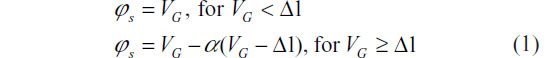
where φs is the channel potential, VG is the gate bias, α is the slope of the drain current curve, and Δ1 is the equilibrium sub-band minima of the first sub-band.
In order to remove the discontinuity at Δ1, the following equation is proposed:13
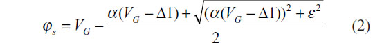
with ε serving as a smoothing parameter (typically around 0.5 V).
The slope of the characteristic curve, α, is expressed as a polynomial of VSD such that α = α0 + α1VSD + α2VSD2, where α0, α1, and α2 are dependent on both CNTFET diameter, d, and gate oxide thickness, tox.14 The drain current, ISD, can now be determined by the simplified expression below:

where

and

thermal voltage

where VTH is the threshold voltage, k is the Boltzmann constant, q the electron charge, and T the temperature.
Hysteretic effects cause a shift of the threshold voltage, which may be considered as the first sub-band, Δ1. Experimentally, a sweep to large positive values of VG creates a positive shift in the threshold voltage,15–17 and VSD does not affect the shift or the position of the curves. According to the variables set forth in the L2P model,5 hysteresis is characterized by a horizontal shift between the two curves, denoted as w, which designates the magnitude of shift around a central voltage, VC, along the horizontal axis. An auxiliary variable, δ, can be used to identify hysteresis orientation. These variables are experimentally obtained. In the case of CNTFETs, without these parameters shown above, the current model cannot show hysteresis. Adapting the threshold voltage to L2P model variables, these effects are evidenced.
Applying these definitions:

with

Although carbon nanotubes are described as having ballistic behavior, the contact resistance between the electrode and the carbon nanotube18 affects the on-state current level because the drain-source voltage in the nanotube is just a fraction of VSD applied to the transistor:

where RCN is the intrinsic resistance for the carbon nanotube, which is determined as h/4q2 (approximately 6.4 kΩ),8 while RD and RS are the drain and source contact resistances, respectively.
Figure 1 illustrates the conceptual procedure for CNTFET modeling, where w and VC are obtained from the L2P model while the other variables arise from the ballistic model.
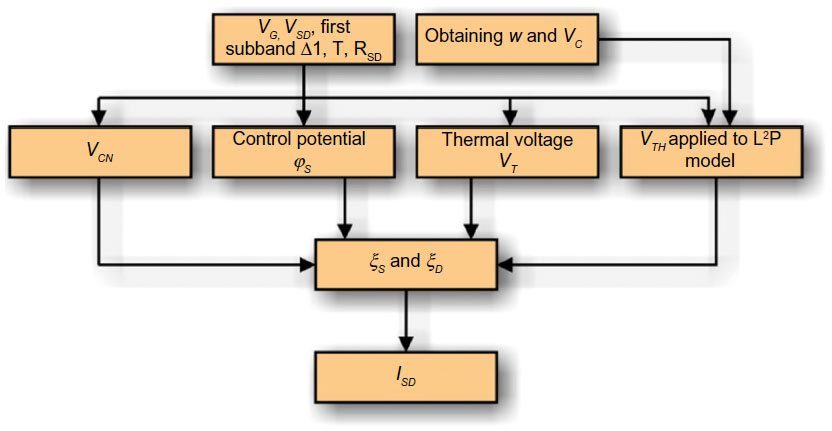 | Figure 1 Flowchart for carbon nanotube field-effect transistor modeling. |
Experimental procedure
Silicon wafers (p-type, orientation <100>, 500–550 μm thickness, 0.001–0.005 Ω·cm resistivity) produced by NOVA Electronic Materials Ltd (Flower Mound, TX, USA) were used in this work. Thin silicon dioxide (SiO2) layers were grown on the wafer by a typical dry–wet–dry oxidation process at a temperature of 1,100°C for 10 minutes, 70 minutes, and 10 minutes, respectively. Prior to the catalyst spinning procedure, the silicon wafer was cut into samples measuring 10×10 mm, which were ultrasonically degreased in trichloroethylene (C2HCl3), acetone ((CH3)2CO), and isopropyl alcohol (C3H8O), rinsed in deionized water, and dried in nitrogen. A solution of ferric nitrate nonahydrate (1.6 mg) + precursor MoO2(acetylacetonate ligand)2 complex (0.5 mg) + aluminum oxide (15 mg) dissolved in methanol (20 mL) was used as the catalyst for carbon nanotube growth. Catalyst islands are patterned, using electron beam lithography and lift-off on boron-doped silicon substrates with 300 nm SiO2 grown by thermal dry oxidation. SWCNTs are grown from these catalyst islands using chemical vapor deposition with a methane and hydrogen gas mixture (total flow 60 sccm) in a 750°C–900°C–750°C three-zone furnace set. The SWCNT samples were grown with methane flow (32 sccm) and hydrogen flow (28 sccm). After imaging as-grown nanotubes with a field-emission scanning electron microscope, source/drain electrodes are patterned by electron beam lithography. The width of the source and drain metal electrodes are 1 μm with a 1.5 μm separation. The metals chromium and gold (thicknesses of 30 Å/1,000 Å) are deposited by sputtering and followed by lift-off in acetone.
Surface morphology of the grown layers was examined by field-emission scanning electron microscopy using a Zeiss SUPRA 55-VP FESEM microscope (Carl Zeiss Meditec AG, Jena, Germany). Micro-Raman spectroscopy was carried out at room temperature using a Renishaw Raman microscope (inVia; Renishaw, Wotton-under-Edge, UK) employing the output of an Ar+ laser (20 mW power) for excitation at λ=514.5 nm. A LabVIEW 2013 SP1 software program (National Instruments Corporation, Austin, TX, USA) was implemented in an IEEE-488 environment, using a computer to control the Model 4140B pA meter/DC voltage source (Hewlett-Packard Inc., Palo Alto, CA, USA), and connected to a four-probe micromanipulator system for characterization of device parameters. All devices were measured at room temperature (300 K) in a controlled pressure (1 atm + 0.12 kPa in H2O) and humidity (30%) environment.
Model parameters identification
For the determination of the L2P model parameters w and VC, we used graphic analysis based on the simulation results. Figure 2 describes the link between these parameters and their visual representation in the theoretical model. w is the horizontal distance between the two curves, obtained by tracing two lines in parallel with the inclination of the curves in their transition regions. Thereafter, VC is obtained by determining the horizontal midpoint of w at the vertical point located in the off-state saturation current value.
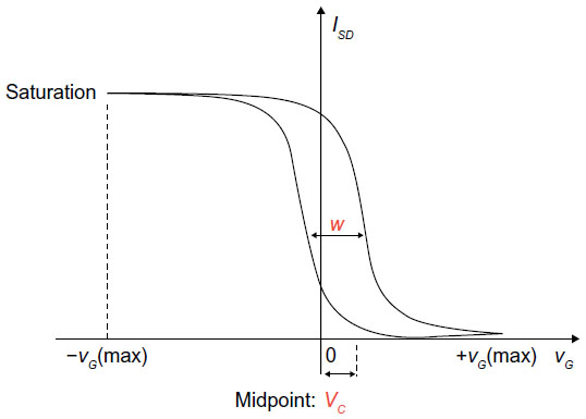 | Figure 2 ISD–VG curves with hysteresis and obtainment of parameters w and VC. |
Although α0, α1, and α2 are inherent to the physical characteristics of the CNTFET, as mentioned in the Model Description section, there is no known mathematical relation that could allow the prior acquisition of these parameters. Thus, we considered each transistor as a stand-alone device, obtaining the slope of the curve in the transition region for each device and drain-source voltage by the minimization of deviations between the data and the model curves in this region. In this way, with at least three measurements of α for different values of VSD, it is possible to determine α0, α1, and α2 for a device by a linear system.
Results and discussion
Figure 3A shows a long and straight single semiconducting nanotube contacted by two gold electrodes to form a CNTFET, and Figure 3B illustrates the typical hysteresis behavior of the nanotube transistor for drain current versus gate voltage (with VSD=0.02 V). Data were taken at room temperature and the device is operated with gate voltages between –10 V< VG <+10 V, in the asymmetric hysteretic transition region. This result corroborates well with the data from a previous work,19 in which the CNTFET also showed that the device conductance was increased for negative gate voltages. We used the ballistic transport model8 and L2P model5 for hysteresis modeling of CNTFETs. Due to the effect complexity, this modeling is susceptible to nonlinearities, so we have incorporated effects in our model to include energy bands, memory phenomena, minor loop accommodation, and stabilization.
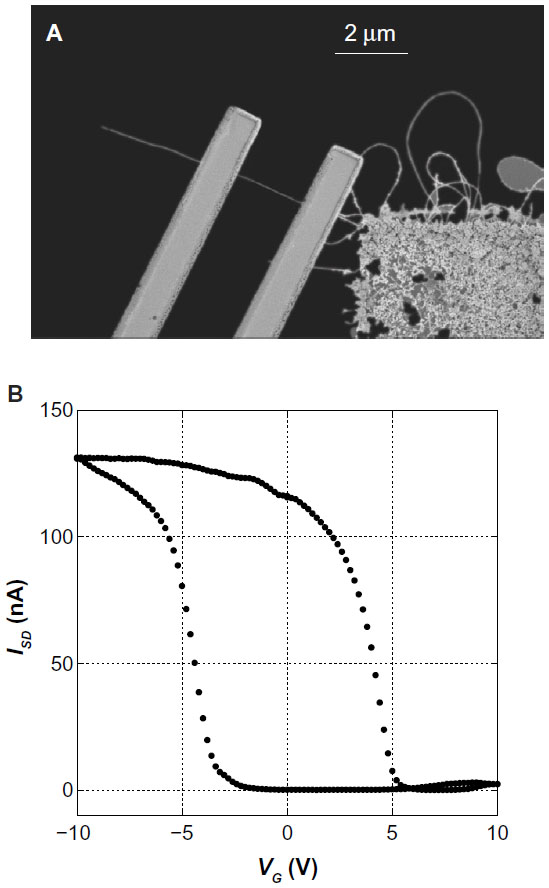 | Figure 3 Fabrication and characterization of CNTFET. |
Figure 4A and B, respectively, show typical Raman spectrum and typical radial breathing mode peaks ranging from 100 to 300 cm–1 that were used to estimate the diameter of the SWCNT.20 We observed two typical SWCNT peaks located at 1,350 cm–1 (D-band) and 1,590 cm–1 (G-band). Table 1 shows details of the diameter distribution of SWCNTs synthesized in the furnace. The diameter distribution of the carbon nanotubes ranged between 1.0 nm and 2.2 nm depending on the different argon concentrations. In order to determine the carbon nanotube diameter, the Raman shift intensities were utilized and, based on the values in the table, we determined the diameter to be 1.0 nm, so that Δ1 was calculated as Δ1~0.45/d (nm) eV.21 Contact resistance was measured in saturation current, and we obtained approximately 100 kΩ in this device.
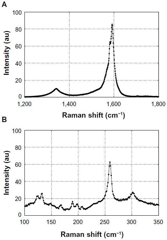 | Figure 4 Raman spectra of the SWCNT. |
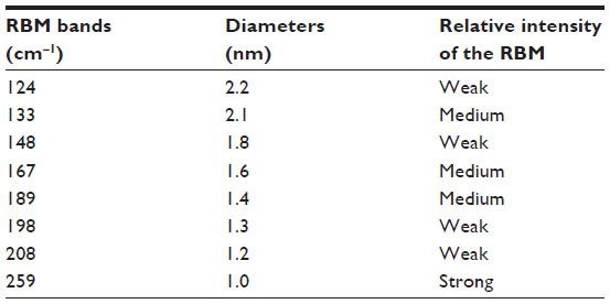 | Table 1 The diameter distribution of single-wall carbon nanotubes synthesized in the furnace |
Simulation was performed at room temperature, using MATLAB (MathWorks, Natick, MA, USA), on the device for different values of VSD and different VG variances. For the device, tox=300 nm and we used fitting parameters α0=0.992, α1=–0.05 V–1 and α2=0.024 V–2.
Figure 5A–C display curve modeling for VG between –2.5 and +2.5 V, –5.0 and +5.0 V, and –10.0 and +10.0 V, respectively, and for VSD equal to 0.03 V, 0.02 V, and 0.01 V. The results highlight how the gate-source voltage sweep affects hysteresis parameters VC and w. A larger sweep enlarges w and shifts VC toward negative values of VG, while changing VSD does not affect these parameters. It is noted that the bottom curves of the model do not reach the same value of the upper curves on negative voltage limit, and the reason we suggest is that the devices did not reach their maximum saturation current, and, for this, the negative voltage limit should be lower. Despite this observation and some inaccuracies due to measurement and parameter deviation, a good fitting could be observed in all graphs.
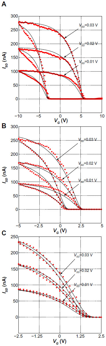 | Figure 5 Comparison between experimental (red dot) and model (line) curves, for VSD=0.03 V, 0.02 V, and 0.01 V. |
This work makes some contributions regarding CNTFET modeling: first, simulations with higher biases of VG were performed, while several articles modeling CNTFET devices used a smaller gate voltage sweep (eg, 0 to +0.05 volts) in simulations, in comparison to our work, and second, the description of hysteresis effect by using L2P parameters showed that hysteretic loop width and shift is sensitive to gate voltage bias.
In order to evaluate the accuracy of the proposed model, three other devices were submitted to measures, for VG between –10 V and +10 V, with the same procedures and conditions described earlier in the “Experimental procedure” section. Subsequently, the experimental results were employed in simulations for the modeling of the devices. Table 2 describes the parameters used for the devices and the relative error of the comparison between the experimental and model curves. It is noted that, with the results shown in Table 2, the model is applicable to other devices with different characteristics and behavior. In spite of the expected relative errors, since the measurement accuracy and model approximations might interfere in the modeling, these differences do not attenuate the effectiveness of the proposed work.
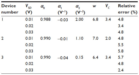 | Table 2 Comparison of parameters and relative error among tested devices |
Conclusion
In this work, we successfully modeled ISD–VG curves including hysteresis effects, for different voltage values and parameters, as a result of mathematical adaptations over the main expression, respecting the physical concepts of ballistic theory. The L2P model contributed to the characterization, as we could use its parameters to distinguish the two curves caused by hysteresis. The modeling brings detailed information about the device behavior, based on its characteristics.
Currently, we are studying improvements in the characterization process. One improvement that we intend to demonstrate in a future work is the prior identification of the hysteretic parameters without using graphic methods. Nonetheless, the significant contribution presented in this article is that, given a device with its parameters, it is possible to mathematically localize a bias point over the experimental curves within a desired region of operation, thereby permitting accurate control of the CNTFET for specific applications, such as nonvolatile memory devices.
Acknowledgments
This work was supported by the CNPq (Process 471864/ 2011-0). The authors (Mateus S Moura and Marcio Fontana) acknowledge the Department of Education (Ministério da Educação, MEC), through the Secretariat of Higher Education (Secretaria de Educação Superior, SESu), for the support of the Tutorial Education Program (Programa de Educação Tutorial, PET) of the Electrical Engineering degree from the Federal University of Bahia (Universidade Federal da Bahia). The authors also thank P Barbara for insightful discussions on hysteresis.
Disclosure
The authors report no conflicts of interest in this work.
References
Pushkarna A, Raghavan S, Mahmoodi H, ed. Comparison of performance parameters of SRAM designs in 16 nm CMOS and CNTFET technologies. SOC Conference (SOCC), 2010 IEEE International; September 27–29, 2010; Las Vegas, NV: SOCC; 2010. | |
Guo J, Datta S, Lundstrom M, et al, ed. Assessment of silicon MOS and carbon nanotube FET performance limits using a general theory of ballistic transistors. International Electron Devices Meeting, 2002. IEDM ’02. International; December 8–11, 2002; San Francisco, CA: The Institute of Electrical and Electronics Engineers; 2002. | |
Tans SJ, Verschueren ARM, Dekker C. Room-temperature transistor based on a single carbon nanotube. Nature. 1998;393:49–52. | |
Robert-Peillard A, Rotkin SV. Modeling hysteresis phenomena in nanotube field-effect transistors. IEEE Trans Nanotechnol. 2005;4(2):284–288. | |
de Almeida LAL, Deep GS, Lima AMN, Neff H. Limiting loop proximity hysteresis model. IEEE Trans Magn. 2003;39(1):523–528. | |
Mayergoyz ID. Mathematical Models of Hysteresis. New York, NY: Springer-Verlag; 1991. | |
Jiles DC, Atherton DL. Ferromagnetic hysteresis. IEEE Trans Magn. 1983;19(5):2183–2185. | |
Raychowdhury A, Mukhopadhyay S, Roy K. A circuit-compatible model of ballistic carbon nanotube field-effect transistors. IEEE Transactions on Computer-Aided Design of Integrated Circuits and Systems. 2004;23(10):1411–1420. | |
Lundstrom M, Ren Z, Datta S. Essential physics of carrier transport in nanoscale MOSFETs. IEEE Trans Electron Devices. 2002;49(1):133–141. | |
Javey A, Guo J, Wang Q, Lundstrom M, Dai H. Ballistic carbon nanotube field-effect transistors. Nature. 2003;424:654–657. | |
Dai H, Javey A, Pop E, Mann D, Kim W, Lu Y. Electrical transport properties and field-effect transistors of carbon nanotubes. Nano: Brief Reports and Reviews. 2006;1(1):1–13. | |
Yang Y, Fedorov G, Barbara P, et al. Coherent nonlocal transport in quantum wires with strongly coupled electrodes. Physical Review B Condensed Matter and Materials Physics. 2013;87(4). | |
Pregaldiny F, Lallement C, Kammerer J. Design-oriented compact modes for CNTFETs. DTIS 2006. International Conference on Design and Test of Integrated Systems in Nanoscale Technology; September 5–7, 2006; Tunis, Tunisia: The Institute of Electrical and Electronics Engineers, 2007. | |
Aouaj A, Bouziane A, Nouacry A. Nanotube carbon transistor (CNTFET), I-V and C-V, a qualitative comparison between fettoy simulator and compact model. ICMCS ’09. International Conference on Multimedia Computing and Systems; April 2–4, 2009; Ouarzazate, Morocco: 236–239. | |
Fuhrer MS, Kim BM, Durkop T, Brintlinger T. High-mobility nanotube transistor memory. Nano Lett. 2002;2(7):755–759. | |
Di Bartolomeo A, Rinzan M, Boyd AK, et al. Electrical properties and memory effects of field-effect transistors from networks of single- and double-walled carbon nanotubes. Nanotechnology. 2010;21(11):115204. | |
Di Bartolomeo A, Yang Y, Rinzan M, Boyd AK, Barbara P. Record endurance for single-walled carbon nanotube-based memory cell. Nanoscale Res Lett. 2010;5(11):1852–1855. | |
Tersoff J. Contact resistance of carbon nanotubes. Appl Phys Lett. 1999;74(15):2122–2124. | |
Zhou J, Barbara P, Paranjape M. Novel in-situ decoration of single-walled carbon nanotube transistors with metal nanoparticles. J Nanosci Nanotechnol. 2010;10(6):3890–3894. | |
Dresselhaus MS, Dresselhaus G, Saito R, Jorio A. Raman spectroscopy of carbon nanotubes. Phys Rep. 2005;409(2):47–99. | |
McEuen PL, Fuhrer MS, Park H. Single-walled carbon nanotube electronics. IEEE Trans Nanotechnol. 2002;1(1):78–85. |
 © 2014 The Author(s). This work is published and licensed by Dove Medical Press Limited. The
full terms of this license are available at https://www.dovepress.com/terms
and incorporate the Creative Commons Attribution
- Non Commercial (unported, 3.0) License.
By accessing the work you hereby accept the Terms. Non-commercial uses of the work are permitted
without any further permission from Dove Medical Press Limited, provided the work is properly
attributed. For permission for commercial use of this work, please see paragraphs 4.2 and 5 of our Terms.
© 2014 The Author(s). This work is published and licensed by Dove Medical Press Limited. The
full terms of this license are available at https://www.dovepress.com/terms
and incorporate the Creative Commons Attribution
- Non Commercial (unported, 3.0) License.
By accessing the work you hereby accept the Terms. Non-commercial uses of the work are permitted
without any further permission from Dove Medical Press Limited, provided the work is properly
attributed. For permission for commercial use of this work, please see paragraphs 4.2 and 5 of our Terms.