")
Back to Journals » International Journal of Nanomedicine » Volume 15
Short Communication: An Updated Design to Implement Artificial Neuron Synaptic Behaviors in One Device with a Control Gate
Authors Qi S, Hu Y, Dai C, Chen P, Wu Z, Webster TJ , Dai M
Received 18 July 2019
Accepted for publication 28 May 2020
Published 20 August 2020 Volume 2020:15 Pages 6239—6245
DOI https://doi.org/10.2147/IJN.S223651
Checked for plagiarism Yes
Review by Single anonymous peer review
Peer reviewer comments 3
Editor who approved publication: Prof. Dr. Anderson Oliveira Lobo
Shaocheng Qi,1 Yongbin Hu,1 Chaoqi Dai,1 Peiqin Chen,1 Zhendong Wu,1 Thomas J Webster,2 Mingzhi Dai1,3
1Ningbo Institute of Materials Technology and Engineering, Chinese Academy of Sciences, Ningbo 315201, People’s Republic of China; 2Department of Chemical Engineering, Northeastern University, Boston, MA, USA; 3Center of Materials Science and Optoelectronics Engineering, University of Chinese Academy of Sciences, Beijing 100049, People’s Republic of China
Correspondence: Thomas J Webster Department of Chemical Engineering
Northeastern University, Boston, MA, USA
Email [email protected]
Mingzhi Dai
Ningbo Institute of Materials Technology and Engineering, Chinese Academy of Sciences, Ningbo 315201, People’s Republic of China
Email [email protected]
Background: As a key component in artificial intelligence computing, a transistor design is updated here as a potential alternative candidate for artificial synaptic behavior implementation. However, further updates are needed to better control artificial synaptic behavior. Here, an updated channel-electrode transistor design is proposed as an artificial synapse device; this structure is different from previously published designs by other groups.
Methods: A semiconductor characterization system was used in order to simulate the artificial synaptic behavior and a scanning electron microscope was used to characterize the device structure.
Results: It was found that the electrode added to the transistor channel had a strong impact on the representative transmission behavior of such artificial synaptic devices, such as excitatory postsynaptic current (EPSC) and the paired-pulse facilitation (PPF) index.
Conclusion: These behaviors were tuned effectively and the impact of the channel electrode is explained by the combined effects of the joint channel electrode and conventional gate. The voltage dependence of such oxide devices suggests more capability to emulate various synaptic behaviors for numerous medical and non-medical applications. This is extremely helpful for future neuromorphic computational system implementation.
Keywords: artificial synapse, thin-film transistor, channel-electrode transistor, neuron behavior control
Introduction
In view of common electronic devices, numerous materials, such as silicon-on-insulator (SOI) and nanotubes, can be used.1–4 In addition, numerous papers focused on artificial synapses have been reported, such as two-terminal memristors5 and devices with three-terminals which have been proposed to mimic artificial synapse functions.1,6-10 While memristors have reliability issues or are hard to fabricate,24,25 three-terminal transistors have been developing for several decades and are appropriate for artificial synaptic realization.16,26 Presynaptic spikes could be emulated by voltage pulses applied on the gate electrode, while the synaptic weight is represented by channel conductance. Typical synaptic behaviors, including excitatory postsynaptic current (EPSC) and paired-pulse facilitation (PPF), have been reported.
The traditional method uses CMOS-based transistors (Metal-Oxide-Semiconductor Field-Effect Transistor, MOSFET) to emulate an artificial synaptic signal; however, the MOSFET synapse needs several transistors to emulate one signal and the energy dissipation of a MOSFET synapse is much higher than natural neurons.20,27 Other synaptic transistors include ferroelectric field-effect transistors28,29 and electric double layer transistors.20,26 Meanwhile, amorphous oxide semiconductor (AOS) materials have attracted much attention due to their optimal properties, including room temperature fabrication conditions, transparency, and electrical properties.1,11 AOS materials such as IGZO (In-Ga-Zn-O) have been reported as resistive change materials in two-terminal resistive-switching memory for artificial synapse emulating.5 The oxygen vacancies in the amorphous oxide semiconductor serve as mobile carriers, which could simulate the mobile ions in real neurons.5,30 Synaptic behaviors from different dimensions have been investigated for the first time in our present design. Two-dimensional presynaptic spikes, which are similar to real life, are of importance and interest to build biological systems, such as neuron synapses.
In this paper, an updated channel-electrode transistor (CET) design is proposed to realize artificial synaptic devices (Figure 1E). The configuration has only one transistor together with an additional electrode jointed in the channel (ie, channel electrode, CE), and a side electrode as the side gate (SG). With a vertically coupled bottom electrode, a channel electrode and a lateral side electrode as the presynaptic terminal, this design could emulate synaptic behaviors in three different directions. It might be helpful to push the development of neuromorphic computation integrated circuits (IC) in the future.31
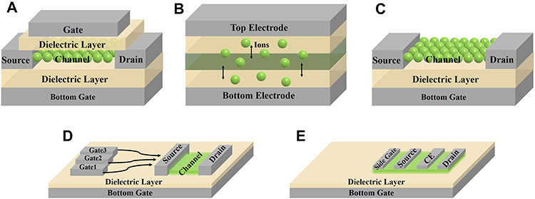 |
Figure 1 3D schematic comparison of the previous structures and our structure. (A) Hybrid heterojunction based synapse.8 (B) Synaptic devices based on ion-exchange kinetics.5,6,9 (C) Electric-double-layer transistor-based synapse.7,10,19 (D) Side gate approach for synaptic behavior control.20 (E) Our channel-electrode transistor (CET) design, with fewer fabrication processes and less area cost. |
Figure 1A–E shows a 3-dimensional schematic comparison among the published designs and our new structure. Some have more layers and the others have more of a footprint than our design. The CET design with a conventional bottom gate and a vertically stacked channel electrode and a lateral side gate could better simulate the synaptic behaviors, which is different from previously published designs by other groups. The electrodes could use conductive materials such as metals and ITO. Here, the control gate uses Ni/Au, which was deposited together with the drain and source electrodes. The CET could be realized with a foundry process at present. Here, we use an amorphous oxide semiconductor (AOS) thin-film transistor (TFT) process12 to realize our CET. The AOS TFTs have many good properties, such as a low-temperature process, high uniformity over large areas and high-stress stability, which suggests wide applications in portable electronics and displays.11,13 IGZO TFTs were used in this study to realize our design.
Experimental Section
For the fabrication, initially, IGZO channels were grown by radio-frequency sputtering on a Si wafer and patterning by lithography, the Si wafer served as the bottom gate and gate dielectric layer. IGZO channels with a 3~36 nm thickness were selected for our investigation here. The channel width and length were about 100 μm and 90–120 μm, respectively, and the dimension of the channel could be decreased by lithography methods and could be as short as a nanometer.14 The thickness of our IGZO semiconductor can be adjusted by tuning the deposition time from 3 nm to 36 nm. The devices with a channel thickness of 3 nm showed stable electrical properties in our experiments.
After the IGZO semiconductor channels were deposited and patterned, the mask patterns of the metal electrodes were transferred to the wafer. Ni/Au metal electrodes (ie, the source, drain, channel electrode, and side electrode) with about a 100 nm thickness were deposited by electron beam evaporation techniques and further developed. The electrode is metal but not limited to metal, and could also be ITO or other conductive materials. Different electrode materials will lead to different experimental results due to their instinctive work function and a different band structure between the electrode and active material. This structure fabrication process, which is typical for a transistor, suggests a good assembly possibly more complex than integrated devices.
Electrical properties were measured by a semiconductor characterization system (Keithley 4200), where the source voltage was set to 0 V and the drain voltage was constant. The pre-synaptic spike was simulated by the voltage applied on the channel electrode (ie, control gate), side gate or the bottom gate. The excitatory postsynaptic current was simulated by the channel current (ie, the current between the drain and source electrode).
Results and Discussion
The synaptic behavior could be obtained by CET with a control gate (Figure 2). In order to obtain the EPSC, a −2 V presynaptic spike was applied to the control gate, which stimulated an EPSC amplitude of over 20 μA. The EPSC reached a peak value and decreased gradually, which is similar to the nonlinear transmission characteristic of a biological synapse.15 It is worth noticing that the EPSC here was obtained on a device with an IGZO layer thickness of only 3 nm, which is shown in the insert in Figure 2A. As the fitting line shown in Figure 2A, the decay of EPSC can be described by a stretched exponential function:
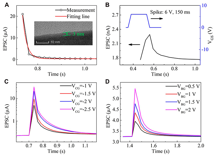 |
Figure 2 EPSC behavior of CET. (A) EPSC triggered by a presynaptic spike on the channel electrode as the control gate, with fitting by a stretched exponential function. Inset is the cross-section of the 3 nm thick IGZO channel layer between the ITO electrodes and the dielectrics layers. (B) EPSC decay experimental behavior triggered by a presynaptic spike on the side gate. (C) EPSC triggered by a presynaptic spike on the control gate with different amplitudes, with a 25 ms pulse width. This shows the control gate could show EPSC without a bottom gate. (D) EPSC triggered by a presynaptic spike on the bottom gate with different amplitudes, with a 25 ms pulse width. |
where τ is the retention time, t0 is the time when the presynaptic spike finishes, I0 is the triggered EPSC, and I∞ is the postsynaptic current at the end of the presynaptic spike. The τ is estimated to be ~2 μs, which means the feature time of the mobile carrier migration is about 2 μs. This representative artificial synaptic transmission behavior is due to the mobile carriers in the amorphous oxide, which depends on the oxide components,1,22 which is similar to those in cation transport among neurons. The oxygen vacancies in the IGZO channel layer serve as the majority carriers, and the artificial synaptic transmission behavior is due to oxygen ion migration and diffusion.5,30
The synaptic behavior of CET could be obtained with a side electrode as the side gate (Figure 2B). When stimulated by a 6 V and 150 ms width spike, an EPSC amplitude of over 2.2 nA was obtained. As shown in Figure 2B, the energy dissipation was 5 pJ, which is on the same order of the aim of power dissipation for neuromorphic systems and much lower than the reported CMOS-based artificial synapse.16,21,32 Here, both the width and length of our sample were on the order of 100 μm. Given a smaller dimension, the current and thus the power dissipation could be reduced. A postsynaptic neuron could be triggered to establish a dynamic logic by the spatiotemporally correlated stimuli from various neurons.
As shown in Figure 2B, the EPSC was controlled under the same voltage by the side gate and was much lower than that by the control gate in Figure 2A. This is consistent with the mechanism for the different structures, with the side gate adjusting the channel in a far separated location and the control gates directly adding to the channel. As shown in Figure 2C and D, both the control gate and the bottom gate have a more direct impact on the channel than the side gate. The EPSC stimulated by the same voltage on the control gate and bottom gate could reach a peak value of μA level, which is far greater than on the side gate. This suggests that a similar synaptic effect is easier to achieve by applying spikes on both the bottom gate and control gate than on the side gate. A vertical coupled gate (bottom gate and control gate) has a stronger impact on device conductivity and thus on the synaptic behavior than that with a lateral side gate. In the real life, neurons have connections from junctions in various directions. We could also note that the impact of the connections from various directions could be emulated, by adjusting the voltages in both the vertical and lateral dimensions.
The transient current arises from states highly localized in energy and is assumed to follow the function exp(-et),2,3 where e in the function is the emission rate of the carriers and t is the transient time after the pulse. Therefore, e is related to the energy level where the carriers emit. If only one e is given, the curves show obvious deviation. If two e, which are correlated to different gates are given, ie, 1/e1 ~0.5 μs and 1/e2 ~0.2 μs, the calculated curve could be found to fit the transient measurement current well. Therefore, we propose a model for transient current for AOS as follows:
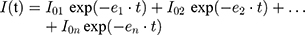
where en corresponds to the No. n gate if there are more than 2 gates and n is the number of the gates which could control the channel including the channel electrodes acting as control gates. This is reasonable for different e corresponding to different gate impacts because it was found that there was an element of localized trap in the deep states, which should have different emission time from the element of the shallow trap in the states near Ec.17 As suggested in Figure 2C and D, both the control gates and the bottom gates could control the EPSC shape. Therefore, there should be at least one additional element to the transient current with another emission time, with a control gate pulse and another bottom/side gate pulse. Therefore, the channel after being turned on should have two emission times for the gate control from the bottom gate, control gate, and other gates. The model for AOS is different from the conventional model.3 This shows that we could adjust the artificial synaptic behaviors on both the amplitude and different transition times.
The mobile carriers in the amorphous oxide depend on the oxide components.1 As shown in Figure 3A, the EPSC was triggered by two successive presynaptic spikes on the control gate with a spike amplitude of 1 V and 1.5 V, the EPSC triggered by the second spike is larger than the first one. The phenomenon is called paired-pulse facilitation (PPF), in which EPSC evoked by the second spike increases when it follows a previous spike closely (25 ms interspike interval here). PPF is a form of short-term synaptic plasticity and is reported to be important for decoding temporal information in the biological system.15 The PPF phenomenon in our CET is due to the oxygen vacancy migration in the IGZO channel layer, when applying a presynaptic spike on the control gate, the oxygen vacancies concentrated near the control gate and diffused slowly into the bulk; when applying the second presynaptic spike, the oxygen vacancies resided near the control gate augmented with the oxygen vacancies triggered by the second spike, thus results in a larger EPSC. The PPF index, ie, the ratio of max EPSC2/max EPSC1, as a function of the interspike interval is shown in Figure 3B. The interspike interval Δtpre is between the two subsequently correlated spikes on the control gate. As seen in Figure 3B, the PPF index reaches a peak value and gradually decreases as the interspike interval increases, the PPF index reaches 1.4 with a Δtpre of 25 ms and could maintain 1.03 after 300 ms. It was found that there is an elevation in responsiveness for the second spike when two spikes are less than 300 ms apart. Therefore, the shorter the Δtpre is, the higher the PPF index would be for a pair of spikes on the control gate, which is consistent with the time-related oxygen vacancy migration. These behaviors were also found in the situation for the bottom gate.
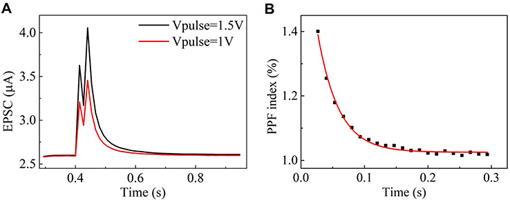 |
Figure 3 (A) Paired-pulse facilitation (PPF) behavior. EPSC triggered by a pair of consecutive spikes at 1 V and 1.5 V, the PPF behavior could be observed. (B) PPF index, ie, the ratio of A2/A1, as a function of interspike interval (presynaptic spike of 1 V, interspike interval from 25 ms to 300 ms). |
Another short-term plasticity behavior is shown in Figure 4A, when stimulated by a series of spikes on the control gate, the channel conductance (ie, synaptic weight) gradually increased and can last for tens of seconds after the spike, which shows a post-tetanic potentiation (PTP) behavior.7,23 The amplitude of the triggered spike is 1.5 V, with a 25 ms pulse width, and an interspike interval of around 50 ms. It is worth mentioning that with this CET structure, long-term potentiation (LTP) behavior could be obtained by changing the channel materials. The synaptic potentiation and depression behaviors are shown in Figure 4B, the EPSC amplitude (ie, synaptic weight) gradually increased when stimulated by sequential positive spikes (1 V, 25 ms), and decreased when following negative spikes (−0.5 V, 25 ms).
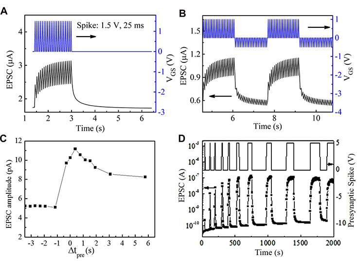 |
Figure 4 (A) CET stimulated by a series of 1.5 V, 25 ms presynaptic spike, the channel conductance increased temporarily, which shows a short-term plasticity behavior. (B) Synaptic potentiation and depression behavior mimicked by a sequential stimulus train. (C) Dynamic logic. EPSC triggered by presynaptic spike 1 and spike 2 on the control gate. (D) Drain current responses to different gate pulses with different amplitudes. |
When two parallel-connected synapses were triggered by a presynaptic spike, the EPSC from different synapses would show a combination effect. The combination would be a dynamic analogue function of time. The EPSC as a function of Δtpre (the interspike interval, Δtpre is the time gap between the two presynaptic spikes when they finished) is shown in Figure 4C. The responses of the post-synapse are measured with a presynaptic spike of 1.5 V and a constant drain voltage VDS of 2 V. When Δtpre=0, the presynaptic spikes applied simultaneously on the two parallel-connected synapses, the EPSCs from the postsynaptic terminal augmented and thus resulted in a combined EPSC, which is larger than the linear sum of EPSC 1 and EPSC 2. This super-linear amplification behavior is similar to what is observed in hippocampal CA1 pyramidal neurons.18
As shown in Figure 4D, the response to the gate pulse of the drain current is similar to the synapse behavior in the nervous system.5 The channel conductance could be adjusted by the voltage pulse duration and amplitude. As shown in Figure 4D, the drain current increases with a presynaptic spike of longer pulse duration, and eventually rose to a maximum. These nonlinear transmission characteristics corresponding to different pulses are very similar to the behaviors of the synapse after the different stimulations in the central nervous system.5 This suggests that the design has the potential ability to realize short-time memory and long-time memory.
Conclusion
In summary, a strategy with a channel electrode is proposed here for artificial synaptic electronics and AI computing. In this strategy, a simplified single-channel transistor, ie, CET, was shown to realize synaptic functions with both a conventional gate and control gates connected to the channel directly. This device, under a driving voltage of no more than 2 V, could be accomplished by standard processes. This study showed that the CET employing advanced semiconductor materials emulated and opened the door for improved neuron behavior control and understanding. This CET device could be appealing for neuromorphic computation circuits as well as other bioinspired applications.
Acknowledgments
This work was supported by the National Natural Science Foundation of China (Grant No. 61574147), Zhejiang Provincial Natural Science Foundation for Distinguished Young Scholar (Grant No. LR17F040002), Ningbo Natural Science Foundation of China (Grant No. 2018A610003), and the Instrument Developing Project of the Chinese Academy of Sciences (Grant No. YJKYYQ20180021).
Disclosure
The authors report no conflicts of interest in this manuscript.
References
1. Fortunato E, Barquinha P, Martins R. Oxide semiconductor thin-film transistors: a review of recent advances. Adv Mater. 2012;24:2945–2986.
2. Yan H, Choe HS, Nam SW, et al. Programmable nanowire circuits for nanoprocessors. Nature. 2011;470:240–244. doi:10.1038/nature09749
3. Bachtold A, Hadle P, Nakanishi T, Dekker C. Logic circuits with carbon nanotube transistors. Science. 2011;294:1317–1320. doi:10.1126/science.1065824
4. Ouyang M, Huang J-L, Cheung CL, Lieber CM. Energy gaps in” metallic” single-walled carbon nanotubes. Science. 2001;292:702–705. doi:10.1126/science.1058853
5. Wang ZQ, Xu HY, Li XH, Yu H, Liu YC, Zhu XJ. Synaptic learning and memory functions achieved using oxygen ion migration/diffusion in an amorphous InGaZnO memristor. Adv Funct Mater. 2012;22:2759–2765. doi:10.1002/adfm.201103148
6. Wu CX, Kim TW, Choi HY, Strukov DB, Yang JJ. Flexible three-dimensional artificial synapse networks with correlated learning and trainable memory capability. Nat Commun. 2017;8:752. doi:10.1038/s41467-017-00803-1
7. Yang JT, Ge C, Du JY, et al. Artificial synapses emulated by an electrolyte-gated tungsten-oxide transistor. Adv Mater. 2018;30:1801548. doi:10.1002/adma.201801548
8. Wang SY, Chen CS, Yu ZH, et al. A multi-input light-stimulated synaptic transistor for complex neuromorphic computing. Adv Mater. 2019;31:1806227. doi:10.1002/adma.201806227
9. Liu QZ, Liu YH, Li J, et al. Fully printed all-solid-state organic flexible artificial synapse for neuromorphic computing. ACS Appl Mater Interfaces. 2019;11:16749–16757. doi:10.1021/acsami.9b00226
10. Zhong YN, Wang T, Gao X, Xu JL, Wang SD. Synapse-like organic thin film memristors. Adv Funct Mater. 2018;28:1800854. doi:10.1002/adfm.201800854
11. Nomura K, Ohta H, Takagi A, Kamiya T, Hirano M, Hosono H. Room-temperature fabrication of transparent flexible thin-film transistors using amorphous oxide semiconductors. Nature. 2004;432:488–492. doi:10.1038/nature03090
12. Hsieh H, Kamiya T, Nomura K, Hosono H, Wu C. Modeling of amorphous thin film transistors and their subgap density of states. Appl Phys Lett. 2008;92:133503. doi:10.1063/1.2857463
13. Jeon S, Ahn S-E, Song I. Gated three-terminal device architecture to eliminate persistent photoconductivity in oxide semiconductor photosensor arrays. Nat Mater. 2012;11:301–305. doi:10.1038/nmat3256
14. Indiveri G, Linares-Barranco B, Legenstein R, Deligeorgis G, Prodromakis T. Integration of nanoscale memristor synapses in neuromorphic computing architectures. Nanotechnology. 2013;24:384010. doi:10.1088/0957-4484/24/38/384010
15. Buonomano DV, Maass W. State-dependent computations: spatiotemporal processing in cortical networks. Nat Rev Neurosci. 2009;10:113–125. doi:10.1038/nrn2558
16. Kim K, Chen C-L, Truong Q, Shen AM, Chen Y. A carbon nanotube synapse with dynamic logic and learning. Adv Mater. 2013;25:1693–1698. doi:10.1002/adma.201203116
17. Dhoot AS, Israel C, Moya X, Mathur ND, Friend RH. Large electric field effect in electrolyte-gated manganites. Phys Rev Lett. 2009;102:136402. doi:10.1103/PhysRevLett.102.136402
18. Yoneyama M, Fukushima Y, Tsukada M, Aihara T. Spatiotemporal characteristics of synaptic EPSP summation on the dendritic trees of hippocampal CA1 pyramidal neurons as revealed by laser uncaging stimulation. Cogn Neurodyn. 2011;5:333–342. doi:10.1007/s11571-011-9158-9
19. Zhou J, Liu N, Zhu L, Shi Y, Wan Q. Energy-efficient artificial synapses based on flexible IGZO electric-double-layer transistors. IEEE Electron Device Lett. 2015;36:198–200. doi:10.1109/LED.2014.2381631
20. Liu YH, Zhu LQ, Feng P, Shi Y, Wan Q. Freestanding artificial synapses based on laterally proton-coupled transistors on chitosan membranes. Adv Mater. 2015;27:5599–5604. doi:10.1002/adma.201502719
21. Azghadi MR, Linares-Barranco B, Abbott D, Leong PHW. A hybrid CMOS-memristor neuromorphic synapse. IEEE Trans Biomed Circuits Syst. 2017;11:434–445. doi:10.1109/TBCAS.2016.2618351
22. Kim H, Moon JY, Heo Y-W, Lee HS. Effect of thermal annealing on Ni/Au contact to a-InGaZnO films deposited by dc sputtering. Thin Solid Films. 2010;518:6348–6351. doi:10.1016/j.tsf.2010.02.054
23. Regehr WG. Short-term presynaptic plasticity. Cold Spring Harb Perspect Biol. 2012;4(7):a005702–a005702. doi:10.1101/cshperspect.a005702
24. Sung C, Hwang H, Yoo IK. Perspective: a review on memristive hardware for neuromorphic computation. J Appl Phys. 2018;124:151903. doi:10.1063/1.5037835
25. Wang J, Zhuge F. Memristive synapses for brain-inspired computing. Adv Mater Technol. 2019;4:1800544. doi:10.1002/admt.201800544
26. Lai Q, Zhang L, Li Z, Stickle WF, Williams RS, Chen Y. Ionic/electronic hybrid materials integrated in a synaptic transistor with signal processing and learning functions. Adv Mater. 2010;22:2448–2453. doi:10.1002/adma.201000282
27. Lau KT, Lee ST. A programmable CMOS gaussian synapse for analogue VLSI neural networks. Int J Electron. 1997;83:91–98. doi:10.1080/002072197135689
28. Oh S, Kim T, Kwak M, et al. HfZrOx-based ferroelectric synapse device with 32 levels of conductance states for neuromorphic applications. IEEE Electron Device Lett. 2017;38:732–735. doi:10.1109/LED.2017.2698083
29. Nishitani Y, Kaneko Y, Ueda M, Morie T, Fujii E. Three-terminal ferroelectric synapse device with concurrent learning function for artificial neural networks. J Appl Phys. 2012;111:124108. doi:10.1063/1.4729915
30. Dai M, Wang W, Wang P, et al. Realization of tunable artificial synapse and memory based on amorphous oxide semiconductor transistor. Sci Rep. 2017;7:10997. doi:10.1038/s41598-017-04641-5
31. Lee Y, Lee TW. Organic synapses for neuromorphic electronics: from brain-inspired computing to sensorimotor nervetronics. Acc Chem Res. 2019;52:964–974. doi:10.1021/acs.accounts.8b00553
32. Xu W, Min S-Y, Hwang H, Lee T-W. Organic core-sheath nanowire artificial synapses with femtojoule energy consumption. Sci Adv. 2016;2:e1501326. doi:10.1126/sciadv.1501326
 © 2020 The Author(s). This work is published and licensed by Dove Medical Press Limited. The full terms of this license are available at https://www.dovepress.com/terms.php and incorporate the Creative Commons Attribution - Non Commercial (unported, v3.0) License.
By accessing the work you hereby accept the Terms. Non-commercial uses of the work are permitted without any further permission from Dove Medical Press Limited, provided the work is properly attributed. For permission for commercial use of this work, please see paragraphs 4.2 and 5 of our Terms.
© 2020 The Author(s). This work is published and licensed by Dove Medical Press Limited. The full terms of this license are available at https://www.dovepress.com/terms.php and incorporate the Creative Commons Attribution - Non Commercial (unported, v3.0) License.
By accessing the work you hereby accept the Terms. Non-commercial uses of the work are permitted without any further permission from Dove Medical Press Limited, provided the work is properly attributed. For permission for commercial use of this work, please see paragraphs 4.2 and 5 of our Terms.