")
Back to Journals » International Journal of Nanomedicine » Volume 14
Change Of Nano Material Electrical Characteristics For Medical System Applications
Authors Chen P, Zhang X, Jiang K, Zhang Q, Qi S, Man W, Webster TJ , Dai M
Received 10 May 2019
Accepted for publication 27 July 2019
Published 27 December 2019 Volume 2019:14 Pages 10119—10122
DOI https://doi.org/10.2147/IJN.S215244
Checked for plagiarism Yes
Review by Single anonymous peer review
Peer reviewer comments 3
Editor who approved publication: Prof. Dr. Anderson Oliveira Lobo
Peiqin Chen,1,2 Xingye Zhang,2 Kemin Jiang,2 Qiang Zhang,2 Shaocheng Qi,2 Weidong Man,1 Thomas J Webster,3 Mingzhi Dai2
1Hubei Key Laboratory of Plasma Chemistry and Advanced Materials, Wuhan Institute of Technology, Wuhan, People’s Republic of China; 2Ningbo Institute of Material Technology and Engineering, Chinese Academy of Sciences, Ningbo, People’s Republic of China; 3Department of Chemical Engineering, Northeastern University, Boston, MA, USA
Correspondence: Thomas J Webster
Department of Chemical Engineering, Northeastern University, Boston, MA 02115, USA
Tel +1-617-373-6585
Email [email protected]
Mingzhi Dai
Ningbo Institute of Material Technology and Engineering, Chinese Academy of Sciences, Ningbo 315201, People’s Republic of China
Tel +86 151 5831 3993
Email [email protected]
Abstract: Amorphous nano oxides (AO) are intriguing advanced materials for a wide variety of nanosystem medical applications including serving as biosensors devices with p-n junctions, nanomaterial-enabled wearable sensors, artificial synaptic devices for AI neurocomputers and medical mimicking research. However, p-type AO with reliable electrical properties are very difficult to obtain according to the literature. Based on the oxide thin film transistor, a phenomenon that could change an n-type material into a p-type semiconductor is proposed and explained here. The typical In-Ga-Zn-O material has been reported to be an n-type semiconductor, which can be changed by physical conditions, such as in processing or bias. In this way, here, we have identified a manner to change nano material electrical properties among n-type and p-type semiconductors very easily for medical application like biosensors in artificial skin.
Keywords: electrical properties, ntype semiconductor, ptype semiconductor, currentvoltage, IV, capacitancevoltage, CV, sensors
Corrigendum for this paper has been published.
Introduction
Since Nomura first published In-Ga-Zn-O (IGZO) thin-film transistors (TFTs) with a reliable electrical performance, amorphous nano oxide (AO) TFTs have attracted extensive attention all over the world for different applications including serving as photovoltaic devices with n-type layers, artificial intelligence (AI), neurocomputing and medical applications.1–8 They have many optimal properties, such as low-temperature processing, high uniformity over large areas and high stress stability, which suggests wide applications in portable electronics and medical displays.
AO materials have stimulated wide attention among chemists, physicists, biologists and mechanical engineers. Such flexible and transparent nano materials with mobile charges can provide for a wide diverse number of medical applications including serving as micro/nano-systems for photovoltaic devices and nanomaterial-enabled wearable sensors or artificial synaptic devices for AI neurocomputers and medical mimicking research.1,5–9
However, most AO are n-type semiconductors. The difficulty in changing their properties limits AO device applications, such as logic gate digital circuits. There are only a few p-type AO with electrical properties comparable to n-type,1 such as Barros et al who prepared a p-type SnO with an oxygen flow of 12.5 sccm,10 and the p-type SnO was also obtained by using a fluorine plasma treatment,11 but p-type IGZO is very rare.
Here, we report an interesting result that the typical n-type AO IGZO, can be changed from an n-type to p-type semiconductor material in a simple way. In this way, the properties of AO TFTs can be better controlled and extended, which facilitates numerous additional medical applications.
Materials And Methods
As shown in Figure 1A, the schematic of the sample includes a typical bottom gate TFT structure. The Si substrate was used as the bottom gate. The nano SiO2 was 100 nm thick as the dielectric layer. The channel was 30 ~ 50 nm thick IGZO which was deposited by a magnetron radio-frequency (RF) sputtering method. We have two different processing conditions for the different samples and the specific parameters are shown in Table 1. Afterwards, the metal electrode Ti/Au was deposited on both processes, using electron-beam evaporation methods. The thickness was on the order of 10 nm.
 |
Table 1 Sample Preparation Process Parameters |
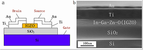 |
Figure 1 (A) 2D schematic of the sample, with the channel as an In-Ga-Zn-O (IGZO) semiconductor. (B) SEM of the cross-section of IGZO transistors, with Si as the bottom gate, SiO2 as the dielectric layer, IGZO as the semiconductor channel layer, and Au/Ti as the top metal electrode layer. |
SEM (Scanning Electron Microscope), drain current-voltage (I-V) measurements and capacitance-voltage (C-V) measurements were performed in order to investigate the physical and electrical properties of the IGZO TFTs. The SEM of the cross-section structure of the sample is shown in Figure 1B.
Results And Discussion
As shown in the I-V and C-V measurements in Figures 2 and 3, the I-V and C-V measurements can indicate whether the semiconductor is n-type or p-type. As shown in the figure, sample No. 1 showed typical I-V and C-V curve characteristics of a n-type semiconductor, while sample No. 2 showed typical I-V and C-V curve characteristics of a p-type semiconductor after being placed for 12 hrs.
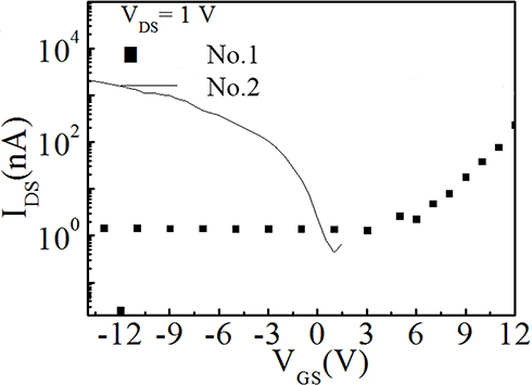 |
Figure 2 The I-V curve of the present n-type TFTs could be easily changed to that of p-type TFTs. |
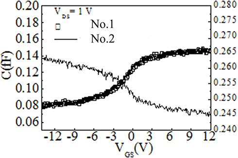 |
Figure 3 The C-V curve of the present n-type TFTs could be easily changed to that of p-type TFTs. |
This phenomenon could be explained as follows: when oxygen is sputtered and deposited on the substrate, it is involved in the channel semiconductor, the oxygen vacancy, which would exist as singly ionized, V+, and doubly ionized states.2,3 Therefore, there would be more positive charge carriers existing in the semiconductor channel, similar to a p-type material.
This mechanism was further studied. The XPS curves of the samples were obtained in the same measurement conditions as follows. At first, the XPS (X-ray photoelectron spectroscopy) data was recorded in the spectrometer in room temperature under high vacuum conditions. Afterwards, the XPS spectra were calibrated relative to the reference energy value of the carbon 1 score level at 284.8 eV. Thirdly, through using Gaussian-Lorentzian (30% Lorentzian) line shapes, the XPS spectral peaks were fitted using Vision Processing 2.3.0 Beta Software. With the help of the Shirley method, the residual background was removed. The two peaks were assigned identical FWHM (full width at half maximum of the peak) values. The XPS spectra was fitted by assuming no chemical shift in the In-O bond during sample preparation. This is a typical assumption to fit the XPS spectra. According to the comparisons of the peak FWHM (full width at half maximum of the peak) and peak position to the standard handbook of XPS, different species could be defined.12 We identified that the different species maybe include In-O bonds.
In Figure 4, XPS characterization of our samples with the IGZO channel suggests In/O>1:1, therefore, oxygen deficiency in the IGZO exists. The channel with additional metal ions is a p-channel, which is similar with previous publications.13,14 Therefore, we could obtain bipolar materials by adding process differences in material properties.
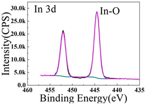 |
Figure 4 XPS of the present TFT channel, which shows different peak values at different binding energies. |
As shown in Figure 5, when the device was under a frequency as small as 20 KHz, there is a significant increase in capacitance as VGS increases, which is similar to the typical C-V curve of a p-type semiconductor. This might be attributed to some of the mobile photons which do not follow the higher frequency measurement. Therefore, the device could become both an n-type and a p-type semiconductor material. A similar phenomenon can be observed not only in nano oxide semiconductors but also in other semiconductor nano materials, such as Si.
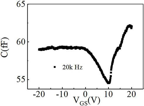 |
Figure 5 The C-V curve of the present p-type IGZO TFTs. |
Conclusion
At present, there are very few p-type semiconductors available, mainly SnOX, NiOX, etc., but we propose here a very simple method to change a very typical n-type amorphous oxide, IGZO, into p-type. Therefore, we might have a device, such as temperature sensors in artificial skin, that uses pure amorphous nano oxide materials, or nano oxide materials like IGZO, which could have an optimal interface between layers due to minor lattice mismatch. In this way, the material properties and, thus, medical applications could be easily extended for additional nanosystems and AI effectively and significantly from the results of this study.
Acknowledgments
This work was supported by the National Natural Science Foundation of China (Grant No. 61574147), Zhejiang Provincial Natural Science Foundation for Distinguished Young Scholar (Grant No. LR17F040002), and the Instrument Developing Project of the Chinese Academy of Sciences (Grant No. YJKYYQ20180021).
Disclosure
The authors report no conflicts of interest in this work.
References
1. Dai M, Guan J, Song Z. A memory structure with different control gates. Adv Electron Mater. 2018;4(7):1800186. doi:10.1002/aelm.v4.7
2. Nomura K, Ohta H, Takagi A, Kamiya T, Hirano M, Hosono H. Room-temperature fabrication of transparent flexible thin-film transistors using amorphous oxide semiconductors. Nature. 2004;432:488–492. doi:10.1038/nature03090
3. Kimura M, Nakanishi T, Nomura K, Kamiya T, Hosono H. Trap densities in amorphous-InGaZnO4 thin-film transistors[J]. Appl Phys Lett. 2008;92(13):133512. doi:10.1063/1.2904704
4. Kim YM, Jeong KS, Yun HJ, et al. Investigation of zinc interstitial ions as the origin of anomalous stress-induced hump in amorphous indium gallium zinc oxide thin film transistors. Appl Phys Lett. 2013;102(17):173502. doi:10.1063/1.4803536
5. Qiao H, Chen L, Rui T, et al. Fabrication and in vitro/in vivo evaluation of amorphous andrographolide nanosuspensions stabilized by d-α-tocopheryl polyethylene glycol 1000 succinate/sodium lauryl sulfate. Int J Nanomed. 2017;12:1033. doi:10.2147/IJN.S120887
6. Fardanesh A, Zibaie S, Shariati B, et al. Amorphous aggregation of tau in the presence of titanium dioxide nanoparticles: biophysical, computational, and cellular studies. Int J Nanomed. 2019;14:901. doi:10.2147/IJN.S194658
7. Dai M, Wang W, Wang P, Iqbal MZ, Annabi N, Amin N. Realization of tunable artificial synapse and memory based on amorphous oxide semiconductor transistor. Sci Rep. 2017;7(1):10997.
8. Dai M, Dai N. Logic circuit function realization by one transistor. Nano Let. 2012;12(11):5954–5956. doi:10.1021/nl303386b
9. Yao S, Swetha P, Zhu Y. Nanomaterial‐enabled wearable sensors for healthcare. Adv Healthcare Mater. 2018;7(1):1700889. doi:10.1002/adhm.v7.1
10. Barros R, Saji KJ, Waerenborgh JC, et al. Role of structure and composition on the performances of P-Type Tin oxide thin-film transistors processed at low-temperatures. Nanomaterials. 2019;9(3):320.
11. Chen PC, Chiu YC, Zheng ZW, Cheng CH, Wu YH. Influence of plasma fluorination on p-type channel tin-oxide thin film transistors. J Alloys Compd. 2017;707:162–166. doi:10.1016/j.jallcom.2016.11.294
12. XPS Chemical Bonds [homepage on the Internet]. Available from: http://genet.sickkids.on.ca/app.
13. Yan L L, Tao C H, Bo C X, et al. Ambipolar inverters using SnO thin-film transistors with balanced electron and hole mobilities. Appl Phys Lett. 2012;100(26):263502. doi:10.1063/1.4731271
14. Ou C W, Dhananjay Y, Ho Z, et al. Anomalous p-channel amorphous oxide transistors based on tin oxide and their complementary circuits. Appl Phys Lett. 2008;92(12):122113. doi:10.1063/1.2898217
 © 2019 The Author(s). This work is published and licensed by Dove Medical Press Limited. The full terms of this license are available at https://www.dovepress.com/terms.php and incorporate the Creative Commons Attribution - Non Commercial (unported, v3.0) License.
By accessing the work you hereby accept the Terms. Non-commercial uses of the work are permitted without any further permission from Dove Medical Press Limited, provided the work is properly attributed. For permission for commercial use of this work, please see paragraphs 4.2 and 5 of our Terms.
© 2019 The Author(s). This work is published and licensed by Dove Medical Press Limited. The full terms of this license are available at https://www.dovepress.com/terms.php and incorporate the Creative Commons Attribution - Non Commercial (unported, v3.0) License.
By accessing the work you hereby accept the Terms. Non-commercial uses of the work are permitted without any further permission from Dove Medical Press Limited, provided the work is properly attributed. For permission for commercial use of this work, please see paragraphs 4.2 and 5 of our Terms.