")
Back to Journals » International Journal of Nanomedicine » Volume 14
A newly developed transparent and flexible one-transistor memory device using advanced nanomaterials for medical and artificial intelligence applications
Authors Dai M , Hu Y, Huo C, Webster TJ , Guo L
Received 6 January 2019
Accepted for publication 11 March 2019
Published 23 July 2019 Volume 2019:14 Pages 5691—5696
DOI https://doi.org/10.2147/IJN.S200581
Checked for plagiarism Yes
Review by Single anonymous peer review
Peer reviewer comments 2
Editor who approved publication: Prof. Dr. Anderson Oliveira Lobo
Mingzhi Dai1,2, Yongbin Hu,3 Changhe Huo,1 Thomas J Webster,4 Liqiang Guo3
1Ningbo Institute of Materials and Technology Engineering, Chinese Academy of Sciences, Beijing 315201, People’s Republic of China; 2Center of Materials Science and Optoelectronics Engineering, University of Chinese Academy of Sciences, Beijing 100049, China; 3Micro/Nano Science & Technology Center, Jiangsu University, Zhenjiang 212013, People’s Republic of China; 4Northeastern University, Boston, MA, USA
Background: Artificial intelligence (AI) integrated circuits (IC) have memory devices as the key component. Due to more complex algorithms and architectures required by neuroscience and other medical applications, various memory structures have been widely proposed and investigated by involving nanomaterials, such as memristors.
Methods: Due to reliability issues of mass production, the dominant memory devices in many computers are still dynamic random access memory (DRAM). A DRAM has one transistor and one capacitor, and so it contains two devices and requires a more compact design to replace.
Results: A one-transistor memory device which is more compact than DRAM is proposed. As far as the authors know, this is the first/novel flexible and transparent one-transistor memory device without any additional process to make a typical transistor and which is based on polyvinyl alcohol. By using indium-titanium-oxide (ITO) as the metal gate, PVA as the dielectric layer and In-Ga-Zn-O (IGZO) as the channel, the memory is implemented mainly based on amorphous oxides and transparent flexible nanomaterials. The charge storage for the memory function was investigated here and is attributed to the mechanism of charge trapping between the ITO/IGZO junctions. It shows typical artificial synaptic transmission behaviors such as EPSC (excitatory postsynaptic currents).
Conclusion: Such a first flexible and transparent one-transistor memory device based on PVA has one capacitor less than DRAM and could be a potential and promising candidate as an alternative for DRAM, especially in the highly complex AI chips needed for numerous medical applications. The flexible memory nanodevice based on flexible dielectrics such as PVA, which shows typical memory and artificial synaptic behaviors, could also be suitable for portable, flexible, transparent or skin-like medical applications.
Keywords: flexible, transparent, one-transistor memory, micro-nano electronics, artificial intelligence
Introduction
The neuromorphic computing paradigm uses memory devices as a key component.1–3 As the most fundamental component in integrated circuits (IC), memory devices have been widely investigated with numerous updated designs.4–21 Memristors have attracted much attention due to their applications, such as multi-levels and potentials in AI circuits.7 Semi-floating gate memory has been proposed based on 2D materials.9 ReRAM, STT-MRAM and PRAM were also proposed due to some special characteristics including fast speed.1 Nanodevices have been studied also.15 However, these all still encounter reliability issues in mass production and application, and may require advanced nanomaterials or high technology different from the dominant silicon-based technology. For instance, organic memory requires organic materials,3 and a transistor with a semi-floating gate requires 2D materials and additional steps for the semi-floating gate.6 Electrical properties of a memristor are mainly controlled by 2-terminal technology, which is more difficult to control than those of the transistor with mature 3- or 4-terminal technology and high reliability.4 Hence, their applications in real life are still very far from reality due to difficulties to match foundry lines. Traditional dynamic random-access memory (DRAM) is still the dominant memory device in IC.6,8 The main volatile memory is DRAM, with a short programming time on the order of 10 ns and a retention time as short as 64 ms. Here, we propose a simpler memory transistor with simpler processing steps.9 The memory transistor, based on flexible and transparent materials, is proposed for medical applications, with the advantages of a fast programming time comparable to DRAM and much longer retention times. Such memory could be a potential alternative candidate to DRAM for information technology applications.
Meanwhile, numerous nanomaterials (such as nanotubes and 2D flexible materials) have been investigated for memory devices due to their lightweight and improved electrical properties.9–15 In addition, they can be mass produced without high cost, similar to silicon, due to their amorphous properties. One of these amorphous oxide semiconductor (AOS) nanomaterials is In-Ga-Zn-O (IGZO). This is because with a scaling down requirement of modern IC, advanced nanomaterials have become more and more attractive. For instance, the semi-floating gate transistor would involve 2D AOS nanomaterials to introduce more of a junction tunneling effect to enhance memory properties.9 Amorphous oxide semiconductors have been studied due to their attractive properties including transparency, flexibility, and moderate mobility. Further, the artificial synaptic devices based on AOS have been widely studied due to potential applications in AI, neurocomputing, and medicine. For example, representative artificial synaptic transmission behaviors are required to be obtained quantitatively in order to mimic clinical behaviors. In order to mimic transmission behaviors easily, an equation is proposed to facilitate related AI and medical studies. The objective of this study was to propose simplified memory designs with advanced nano materials. Here, our devices are the first artificial synaptic transistors based on a flexible polyvinyl alcohol (PVA) grid insulating layer.
Methods
As shown in Figure 1, the processing of such an updated memory structure could be similar to a transistor. The preparation process of the samples with the bottom gate top contact structure is as follows. On one hand, the transistor has an n-type Si doping on the Si wafer as the bottom gate layer. The SiO2 thickness was about 100 nm. PVA was then grown on the bottom gate layer as the dielectrics layer by spin coating. On the other hand, for the flexible transparent thin film transistors, PET was used as a flexible substrate with ITO on the top as the bottom gate. The gate insulation layer was prepared by PVA. A 10 wt% polyvinyl alcohol solution was prepared by dissolving PVA by magnetic stirring and heating, under atmospheric pressure and room temperature. Afterward, a PVA grid insulating layer was prepared by a spin coating method, first coating at 200 rpm for 3 s, then coating at 2,000 rpm for 20 s. The samples with coated PVA films were then heated at 900°C for 30 min. Different advanced transparent materials (such as PI) were also proposed to play a role as dielectrics, but PVA fits best here. Afterward, an n-type oxide semiconductor, indium gallium zinc oxide (IGZO), was deposited on the PVA as the channel layer. The 35 nm thick channel was formed by magnetron radio-frequency sputtering with designed masks and only the IGZO channels were deposited separately. Parameters of flow rate, sputtering time and pressure were 14 sccm, 5 min, and 0.5 Pa, respectively. The metal electrode layer for the drain and the source of the channel was deposited by electron beam evaporation and masks. The channel widths and lengths were 200 μm and 400 μm, respectively, with a thickness in the nanometer regime to maintain transparency and flexibility attractive for medical applications. The drain and source electrodes have a length and width as 150 μm and 1,000 μm, respectively.
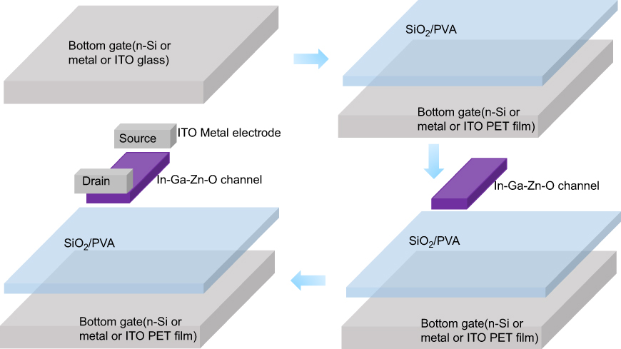 |
Figure 1 Schematic and process flow of the memory based on oxide nanomaterials. |
Results
A top microscope view of the transparent memory transistor is shown in Figure 2. As shown in Figure 2, the top and bottom long transparent lines where the pins probe are the ITO drain and source electrodes, respectively. The transparent section between the drain and the source is the IGZO channel. Figure 2 also shows that the memory transistor is totally transparent and flexible.
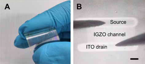 |
Figure 2 (A) A view of the transparent and flexible memory transistor. (B) Top view of the memory transistor with two pins probed on the source and drain electrodes. The channel width is 400 µm, and the length is 200 µm, scale bar=150 μm. |
A typical memory curve is the transfer curve window of the memory transistor,1,12 as shown in Figure 3. The hysteresis loop of the transfer curve is named the memory window. The memory window could be increased by the maximum gate voltage VGSmax. It is shown here that a higher gate voltage VGS could lead to a larger memory window. This is because of an enhanced programming effect. The window could be as large as over 4 V, which is a window large enough for memory function. The initial measurement curves could be repeated in all of the three measurement curves sweeping from a negative VGS to positive VGS, which suggests that the device characteristics show good repeatability. The general difference of the memory window is mainly generated by VGS and is demonstrated on the left part of the memory window where VGS sweeps back from a positive to a negative VGS. It is shown that both the voltage difference range and the current difference range increase with a larger VGS. The reason is that VGS leads to a programming effect of the memory device so that a larger VGS leads to an enhanced memory effect.
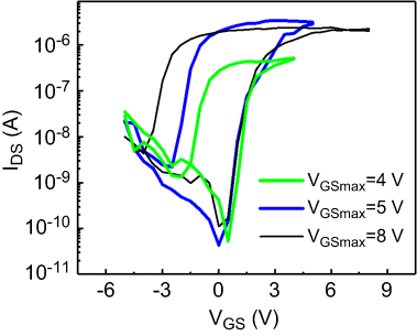 |
Figure 3 Transfer curves of a one memory transistor before and after programming at VDS =1.5 V. |
The programming is as follows. When VGS is positive, the IGZO semiconductor channel is turned on, and there are a lot of mobile electrons along the channel. The electrons are attracted to the ITO drain and source electrodes and stored in the junction between ITO and IGZO. Such electron storage in the ITO/IGZO junction could repel electrons moving them toward the junction on the channel top surface side. This facilitates electron carriers to move towards the channel bottom side near the bottom gate to contribute to the channel current. In this way, the channel current could be enhanced when the same VGS is applied, due to the electron storage into the junction of the ITO/IGZO. When the same VGS is applied, the channel is turned on more easily. When VGSmax increases, the programming effect is enhanced so that the memory window is enlarged.
In addition, as shown in Figure 3, the drain current IDS could be adjusted with VGSmax. As a higher VGSmax is applied, it could lead to a higher IDS at the same VGS when VGS is swept back from positive to negative values. The current on/off contrast, which is also one of the memory properties, could be adjusted from 104 to 105 in the sample data presented here due to different VGSmas. This suggests a multi-level charge storage application, and the value of the memory charge level could be adjusted. The on/off state contrast and hence the retention time after programming could be adjusted by the voltage bias, according to Figure 3. This shows that the memory transistor has a potential application to replace DRAM also. With proper adjustment, such as proper programming conditions and semiconductor materials, the memory current on/off contrast and thus the memory retention time correlating to such contrast could be controlled.
Discussion
The carrier injection into the junction between the layers is the key mechanism behind the memory properties. While there are IGZO and ITO nanomaterials deposited in sequence, a junction is formed between IGZO and ITO. As shown in Figure 3, when VGS <0, the channel is turned off. When VGS >0, IDS >0, ie, the semiconductor channel is turned on. In this case, the transistor using such processing is a nMOS (n-type metal oxide semiconductor) transistor. For a typical nMOS transistor, the majority of carriers are electrons. Therefore, the mobile carriers in the channel are electrons. Figure 4 explains the programming process of such a transparent memory transistor. As shown in Figure 4, when a gate voltage VGS is applied on the Si bottom gate, a drain voltage VDS is applied on the drain, there is a vertical electrical field between the semiconductor junction (ITO-IGZO) layers. When VGS >0 and VDS >0, the electrons are injected into the junction between the ITO electrodes and the channel, and vice versa when VGS <0 and VDS >0. In this way, the programming process in the memory device can be implemented.
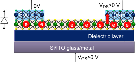 |
Figure 4 Cross section schematic of the one transistor memory programming during IV measurements. |
For ITO-IGZO junctions, it has been previously shown to be one of the fastest speeds reported for memory devices.12 Even with such a short programming time on the order of 10 ns, an obvious current on/off state contrast could be observed after the programming. The programming time on the order of 10 ns is among the fastest programming times.1,12 This is limited by the minimum value of pulse generators (three generators are needed for the pulse voltage for programming applied on the drain control gate and top gate, respectively) and is on the same order of DRAM (10 ns).
In addition, our configuration and one-transistor memory structure could also be used as synapse devices.13–15 Synapse characteristics (such as signal processing functions) named excitatory postsynaptic currents (EPSC) useful for both memory loss and memory retention loss were investigated in our structure.13 As shown in Figure 5A, EPSC reaches a peak value I0 and decreases gradually, which is similar to that in a biological excitatory synapse. A VG spike on the gate generates transient ionic fluxes in the semiconductor layer and an excitatory postsynaptic current EPSC in the transistor drain could be measured. For the 2-terminal measurement, which is a typical synaptic measurement, we can measure EPSC from the drain by applying a spike VG on the gate.15 For 3-terminal measurements, we did the same measurement as with a 2-terminal one by adding the source voltage as 0 V.13 As shown in Figure 3A, power consumption was 5 pJ, which is on the same order of the dissipation aim for a neuromorphic system application.16 Here, the width of our sample is 10 μm. Given a smaller device, power dissipation could be reduced.
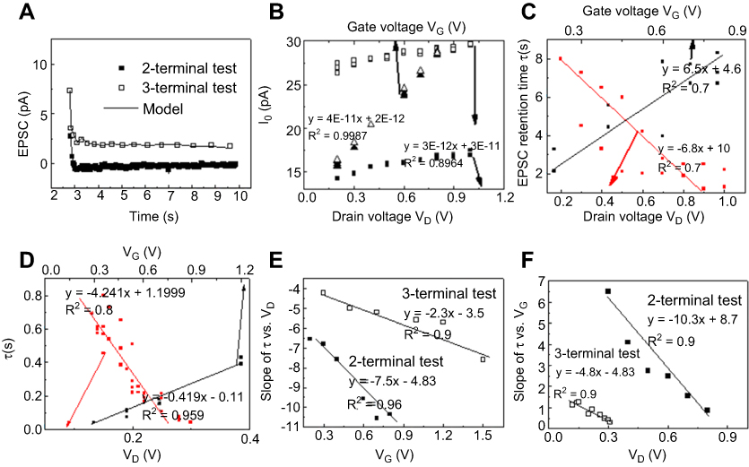 |
Figure 5 EPSC 1 triggered by a presynaptic spike on the bottom gate with 2- and 3-terminal measurements. (A) Eq. (1) fits well with the measurement of both 2- (with a spike on the gate, amplitude as VG, and DC drain voltage VD) and 3-terminal (with a spike on the gate, VD and source voltage VS=0) EPSC. (B) Amplitude in Eq. (1) increases with both VG and VD for 2-terminal measurements. (C) EPSC retention time τ vs voltage for 2-terminal measurements. (D) τ vs voltage for 3-terminal measurements; arrows represent the corresponding y-axis. (E) Dependence of τ-VD slope on VG. (F) Dependence of τ-VG slope on VD. |
As shown in Figure 5A, the decay of EPSC in the 3-terminal samples is generally larger than that in 2-terminal samples. They both can be described by a stretched exponential function:13
(1)
where τ is the retention time, t0 is the time when the presynaptic spike finishes, prefactor I0 is the triggered EPSC at the end of the presynaptic spike, β is the stretch index ranging between 0 and 1, and I∞ is the final current of the EPSC test. As shown in the fittings of Figure 5B–F, I0 and τ show a linear dependence on both gate spike amplitude VG and drain voltage VD, which means that different shapes of EPSC could be obtained easily by adjusting VG and VD.
With these voltage dependence findings, we can easily realize desired synaptic behaviors without changing materials or spike cycles. Figure 5B shows that I0 increases with increasing VD and VG, which could be found in 2- and 3-terminal measurements. Figure 5C and D show that the τ of EPSC was reduced by increasing VD, but increases when VG increases. Figure 5E and F show that the τ-VG slope is impacted by the VD and τ-VD slope by VG. Thus, Eq. (1) can be updated as:
(2) (3) (4) (5)


where a, b, c, d, e, x, y, and z are constants.
With the updated models, complex synaptic device behaviors with different I0 and τ would be emulated easily, including EPSC, and memory loss behaviors including both STM (short term memory) and LTM (long term memory).5,18 The model is based on measurements performed on over 10 samples, and each finding from the trend was repeatable. The quantitative models can give a guideline of how to adjust VG and VD to obtain different synaptic behaviors in a certain voltage range, although the constants need to be adjusted for different processing and devices.
Conclusion
The first transparent and flexible one-transistor design for memory without an additional process to a typical transistor has been proposed and implemented here. It was fabricated using oxide nanomaterials with nanometer thickness attractive for numerous medical applications, such as wearable (or even implantable) sensors. Its window is as large as 4 V with a high current on/off state contrast before and after programming as large as 105. The mechanism of this compact memory is attributed to a junction between the transistor channel and electrode. This memory is likely to be used as alternative memory with quasi-non-volatile memory as an alternative for DRAM in information technology, with its simple design and adjustable electrical properties such as bias-dependent current on/off state contrast and window. This memory structure shows artificial synaptic behaviors and could be used in neuromorphics for artificial intelligence applications. This first transparent and flexible one-transistor design for memory without an additional process to a typical transistor is based on PVA, and could be a potential candidate for electronic skin, portable electronics, artificial intelligence, and sensor applications.
Acknowledgments
This work was supported by the National Science and Technology Major Project of the Ministry of Science and Technology of China (2017YFB03031001), the National Natural Science Foundation of China (Grant No. 61574147), Zhejiang Provincial Natural Science Foundation for Distinguished Young Scholar (Grant No. LR17F040002), Instrument Developing Project of the Chinese Academy of Sciences (Grant No. YJKYYQ20180021), and the Project of the National Natural Science Foundation for Major Research Projects (91648109).
Author contributions
All authors contributed to data analysis, drafting and revising the article, gave final approval of the version to be published, and agree to be accountable for all aspects of the work.
Disclosure
The authors report no conflicts of interest in this work.
References
1. Meena J, Sze S, Chand U, Tseng T. Overview of emerging nonvolatile memory technologies. Nanoscale Res Lett. 2014;9:526. doi:10.1186/1556-276X-9-526
2. Ke Y, Wang S, Liu G, Li M, White T, Long Y. Vanadium dioxide: the multistimuli responsive material and its applications. Small. 2018;14:1802025. doi:10.1002/smll.v14.39
3. Zhou L, Mao J, Ren Y, et al. Biological spiking synapse constructed from solution processed bimetal core-shell nanoparticle based composites. Small. 2018;14:1800288. doi:10.1002/smll.v14.28
4. Luo Y, Chen C, Hong D, He X, Wang J. Thermal-induced dielectric switching with 40K wide hysteresis loop near room temperature. J Phys Chem Lett. 2018;9:2158–2163. doi:10.1021/acs.jpclett.8b00597
5. Martins R, Barquinha P, Pereira L, et al. Write-erase and read paper memory transistor. Appl Phys Lett. 2008;93:203501. doi:10.1063/1.3030873
6. Martins R, Barquinha P, Pereira L, et al. Selective floating gate non-volatile paper memory transistor. Phys Status Solidi-R. 2009;3:308–310. doi:10.1002/pssr.200903268
7. Bernabe L. Memristors fire away. Nat Electron. 2018;1:100. doi:10.1038/s41928-018-0028-x
8. Dennard RH. Field-effect transistor memory. IEEE Solid-State Circuits Newsletter. 2008;13(1):17–25. doi:10.1109/n-ssc.2008.4785686.
9. Liu C, Yan X, Song X, Ding S, Zhang DW, Zhou P. A semi-floating gate memory based on van der Waals heterostructures for quasi-non-volatile applications. Nat Nanotechnol. 2018;13:404. doi:10.1038/s41565-018-0102-6
10. Emin S, Singh SP, Han L, Satoh N, Islam A. Colloidal quantum dot solar cells. Solar Energy. 2011;85:1264–1282. doi:10.1016/j.solener.2011.02.005
11. Dong H, Zhang X, Zhao D, et al. High performance bipolar resistive switching memory devices based on Zn2SnO4 nanowires. Nanoscale. 2012;4:2571. doi:10.1039/c2nr30133d
12. Dai M, Guan J, Song Z. A memory structure with different control gates. Adv Funct Mater. 2018;4:1800186. doi:10.1002/aelm.v4.7
13. Wang Z, Xu HY, Li XH, et al. Synaptic learning and memory functions achieved using oxygen ion migration/diffusion in an amorphous InGaZnO memristor. Adv Funct Mater. 2012;22:2759. doi:10.1002/adfm.v22.13
14. Kim K, Jung YH, Jung WK, et al. Batteries: encapsulated monoclinic sulfur for stable cycling of li-s rechargeable batteries. Adv Mater. 2013;25:1693. doi:10.1002/adma.201370286
15. Lai Q, Zhang L, Li Z, Stickle WF, Williams RS, Chen Y. Ionic/electronic hybrid materials integrated in a synaptic transistor with signal processing and learning functions. Adv Mater. 2010;22:2448. doi:10.1002/adma.v22:22
16. Fancher RE, Rutherford A. Pioneers of Psychology: A History. New York (NY): W. W. Norton & Company, Inc; 2012:357.
17. Wang W, Wang P, Dai M. Simplification of sub-gap density of states extraction method for amorphous In-Ga-Zn-O thin-film transistors by a single capacitance-voltage curve. Microelectron Reliab. 2018;83:111–114. doi:10.1016/j.microrel.2018.01.007
18. Alshammari H, Hota MK, Alshareef HN. Transparent electronics using one binary oxide for all transistor layers. Small. 2018;14:1803969. doi:10.1002/smll.v14.51
19. Ertosun MG, Kapur P, and Saraswat KC. A highly scalable capacitorless double gate quantum well single transistor DRAM: 1T-QW DRAM. IEEE Electron Devices Soc. 2008;29:6. doi:10.1109/led.2008.2007508.
20. Hasegawa T, Itoh Y, Tanaka H, et al. Volatile/nonvolatile dual-functional atom transistor. Appl Phys Express. 2010;4:015204. doi:10.1143/APEX.4.015204
21. Wang Q, Xu HY, Li XH, Yu H, Liu YC, Zhu XJ. Synaptic learning and memory functions achieved using oxygen ion migration/diffusion in an amorphous InGaZnO memristor. Adv Funct Mater. 2012;22:2759–2765. doi:10.1002/adfm.v22.13
 © 2019 The Author(s). This work is published and licensed by Dove Medical Press Limited. The full terms of this license are available at https://www.dovepress.com/terms.php and incorporate the Creative Commons Attribution - Non Commercial (unported, v3.0) License.
By accessing the work you hereby accept the Terms. Non-commercial uses of the work are permitted without any further permission from Dove Medical Press Limited, provided the work is properly attributed. For permission for commercial use of this work, please see paragraphs 4.2 and 5 of our Terms.
© 2019 The Author(s). This work is published and licensed by Dove Medical Press Limited. The full terms of this license are available at https://www.dovepress.com/terms.php and incorporate the Creative Commons Attribution - Non Commercial (unported, v3.0) License.
By accessing the work you hereby accept the Terms. Non-commercial uses of the work are permitted without any further permission from Dove Medical Press Limited, provided the work is properly attributed. For permission for commercial use of this work, please see paragraphs 4.2 and 5 of our Terms.