")
Back to Journals » International Journal of Nanomedicine » Volume 12
A strategy to minimize the sensing voltage drift error in a transistor biosensor with a nanoscale sensing gate
Authors Son HW, Jeun M, Choi J , Lee KH
Received 10 February 2017
Accepted for publication 23 March 2017
Published 11 April 2017 Volume 2017:12 Pages 2951—2956
DOI https://doi.org/10.2147/IJN.S134441
Checked for plagiarism Yes
Review by Single anonymous peer review
Peer reviewer comments 2
Editor who approved publication: Dr Thomas Webster
Hyun Woo Son,1,* Minhong Jeun,1,* Jaewon Choi,1,2 Kwan Hyi Lee1,2
1Center for Biomaterials, Biomedical Research Institute, Korea Institute of Science and Technology, Seoul, 2Department of Biomedical Engineering, Korea University of Science and Technology, Daejeon, Republic of Korea
*These authors contributed equally to this work
Abstract: An ion-sensitive field-effect transistor (ISFET) biosensor is thought to be the center of the next era of health diagnosis. However, questions are raised about its functions and reliability in liquid samples. Consequently, real-life clinical applications are few in number. In this study, we report a strategy to minimize the sensing signal drift error during bioanalyte detection in an ISFET biosensor. A nanoscale SnO2 thin film is used as a gate oxide layer (GOL), and the surface of the GOL is chemically modified for improving bioanalyte-specific binding and for reducing undesirable ion reactions in sample solutions. The ISFET biosensor with surface-modified GOL shows significantly reduced sensing signal error compared with an ISFET with bare GOL in both diluted and undiluted phosphate buffered saline solutions.
Keywords: extended gate, surface treatment, biosensor, SnO2, ISFET
Introduction
The pH-sensing ion-sensitive field-effect transistor (ISFET), first proposed by Bergveld in 1970, has become the basis for many contemporary semiconductors and their respective biosensors.1 In an ISFET, the ions within the sample media undergo multiple environment-influenced reactions. The resulting molecules from these reactions accumulate upon the gate oxide layer (GOL), and the resulting change in charge affects the conductance in the ISFET channel.2,3 Consequently, the conductance between the source and the drain will differ, and this change is expressed as an electrical signal.
The GOLs of ISFETs are usually made up of dielectric materials, such as SnO2,4–7 ZnO,8 SiO2,9,10 Al2O3,11 Si3N4,12,13 Ta2O5,14 TiO2,15 and WO3,16 which readily react with the H+ and OH− of the media. Dielectric materials that have a high reactivity with ions are used as either pH sensor or gas sensor.17 However, because other ions within the sample media also affect the surface charge on the GOL, the electrical characteristics such as the threshold voltage and channel conductance will be influenced.
ISFET-based biosensors, which detect bioanalytes, are affected by the undesirable ions in the media, and the resulting fluctuations or noise may cause the results to be deemed untrustworthy. Although the signal may stabilize as time progresses and the reaction becomes saturated (reaches equilibrium state), the noise factor must be acknowledged when evaluating the final signal. Because the target bioanalyte is already in small amounts inside the target solution, any other factors that may affect the signal, such as the ions within the solution media, will affect the sensitivity of the biosensor. When the biosensor applies highly reactive nanowires and thin films to enhance its sensitivity, the unwanted noise factor may also be increased and affect the result even more.
In this study, we report a strategy to minimize the sensing voltage error in the ISFET biosensor. To improve specific bioanalyte binding and to reduce undesirable ion reactions, an optimal presurface treatment on the gate oxide is demonstrated. In addition, the sensing voltage drift error (ΔVdf) of the ISFET biosensor before presurface treatment and after presurface treatment is analyzed. Finally, because multiple teams that study and utilize the ISFET biosensor dilute the media to obtain a longer Debye screening length, we analyzed the ΔVdf for 1× phosphate buffered saline (PBS) and 0.01× PBS solutions.
Experimental
Sensing gate fabrication
The GOL of an ISFET biosensor was fabricated by depositing an SnO2 (99.9%) thin film on the top of an indium tin oxide (ITO) glass (ITO thickness: 300 nm). The 80 nm SnO2 film was deposited using a radio frequency (RF) magnetron sputtering system (RF power: 50 W, base pressure: 2×10⁻⁶ Torr, work pressure: 18 mTorr, Ar gas flow: 5 sccm). The polydimethylsiloxane (PDMS) block was manufactured from a Sylgard 184 Silicone Elastomer Kit (Dow Corning, Seoul, Republic of Korea), which was composed of a base and a curing agent. The base and curing agent were mixed at a 10:1 ratio and baked at 60°C for 4 h. The PDMS block was then punctured with 6 mm holes to form a sample media reservoir. To attach the PDMS to the surface of GOL, the GOL was sonicated in deionized water for 1 min and then sonicated in ethanol for 1 min. The GOL was then subjected to N2 gas blowing. The PDMS block and GOL were then placed inside an O2 plasma system (CUTE-MPR; Femto Science, Gyeonggi-Do, Republic of Korea) and treated with O2 plasma (DC power: 70 W, time: 1 min, O2 flow: 30 sccm, base pressure: 5×10⁻² Torr, working pressure: 5×10⁻¹ Torr). The PDMS block and GOL were then attached together to form the sensing gate (Figure 1).
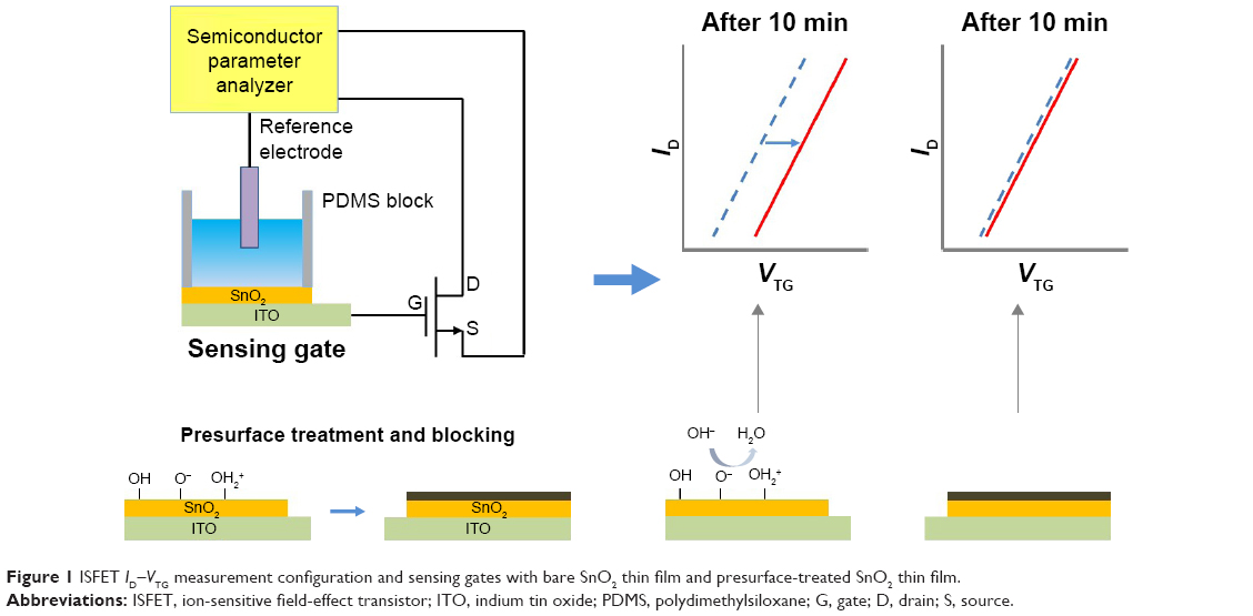 | Figure 1 ISFET ID–VTG measurement configuration and sensing gates with bare SnO2 thin film and presurface-treated SnO2 thin film. |
Presurface treatment of GOL and antibody fixation
The GOL surface of the sensing gate was treated with plasma to form OH functional groups on the reservoir surface. Then, 5% 3-aminopropyltriethoxysilane (APTES) was prepared and quickly added to the surface of the GOL for the formation of NH2 functional groups. After the addition of the APTES, the GOL was placed inside a petri dish and the petri dish was sealed with parafilm for 1 h. The chemical reaction should occur in a dark place. After 1 h, the sensing gate was sonicated in ethanol for 1 min and dried with N2 gas. The sensing gate was baked on a hot plate at 120°C.
To functionalize the GOL surface of the sensing gate with COOH functional groups, 5% 1 M succinic anhydride was made from succinic anhydride powder and dimethyl formamide (DMF) and added onto the surface of the GOL. The petri dish was sealed with parafilm and placed inside an incubator at 37°C for overnight. The presurface-treated sensing gate was washed with DMF and deionized water for 20 s. This GOL was then treated with 1-ethyl-3-(3-dimethylaminopropyl) carbodiimide (EDC) HCL and Sulfo-N-hydroxysulfosuccinimide (NHS) chemistry.18 GOL after the addition of EDC and Sulfo-NHS was identified as a surface-treated GOL (ST-GOL). Antibodies were then added to the wells. Here, we used prostate-specific membrane antigen (PSMA) antibodies. The PSMA antibody was provided by “Biorbyt” (catalog number orb25888; San Francisco, CA, USA). The host of the PSMA antibody was mouse. It had an IgG2b isotype structure and was specific to the c-terminal of a PSMA antigen. The PSMA antibody was conjugated onto the sensing gate surface at a concentration of 100 nM.
To prevent unwanted reactions with unreacted chemical cross-linkers left on the surface, 1 M ethanolamine (pH 8.5) was added. After adding the ethanolamine to the ST-GOL, the ST-GOL was washed with 1× PBS. In order to protect the ST-GOL from nonspecific binding, 10% bovine serum albumin (BSA) was added and left to undergo the chemical reaction for 1 h. Finally, the ST-GOL was washed with 1× PBS (Figure 2).
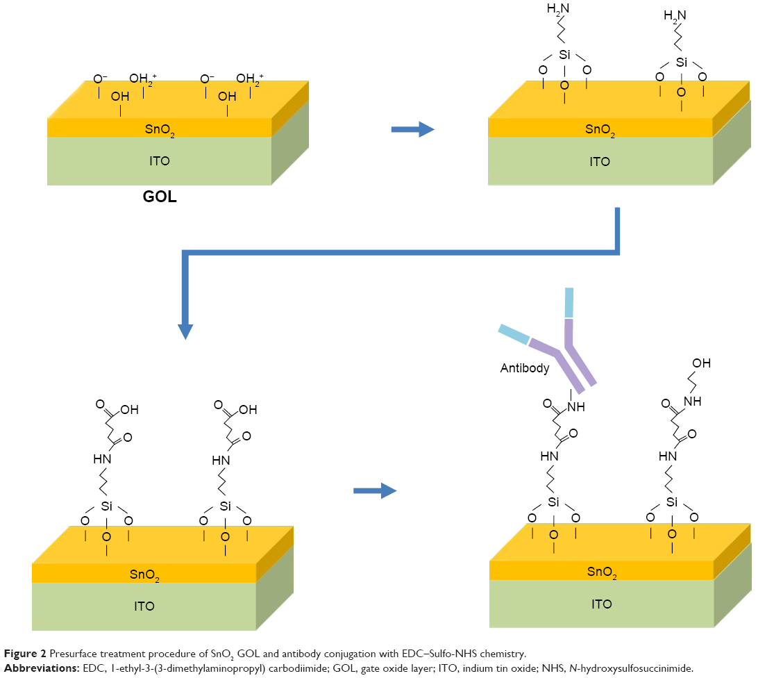 | Figure 2 Presurface treatment procedure of SnO2 GOL and antibody conjugation with EDC–Sulfo-NHS chemistry. |
Measurement
A commercial Ag/AgCl reference electrode (Qrins, MF-2097), a commercial CMOS transistor (ON Semiconductor, MC14007UB, N-type MOSFET), and a high precision semiconductor parameter analyzer (4200-SCS; Keysight Technologies, Santa Rosa, CA, USA) were utilized for the measurement of the ΔVdf.
The experiment was conducted under different conditions. In the initial condition, the ΔVdr of the I–V curves was measured at the 0, 1, 3, and 5 min marks after inserting a 0.01× PBS solution into PDMS reservoirs on all the sensing gates. In the second condition, the 0.01× PBS was replaced with 1× PBS and the solution was added into the PDMS reservoirs on all the sensing gates. The measurement was taken at the same time points as the initial condition (0, 1, 3, and 5 min marks). The chemical compositions of the PBS solution are as follows: 1) potassium phosphate monobasic (KH2PO4) 1.0589 mM, 2) sodium chloride (NaCl) 155.172 mM, and 3) sodium phosphate dibasic (Na2HPO4·7H2O) 2.9665 mM. There is no calcium chloride or magnesium chloride in this buffer. The pH of the PBS is 7.4.
In addition, to measure the ΔVdf difference between the different surface treatments of the GOL, 1× PBS was added to bare GOL, ST-GOL without antibodies, and ST-GOL with antibodies. The ΔVdr was measured at the 0, 1, 3, 5, and 10 min marks (Figure 1).
Results and discussion
We investigated the ΔVdf of a bare GOL, an ST-GOL without antibodies, and an ST-GOL with antibodies in 0.01× PBS (Figure 3A–C). After adding 0.01× PBS into all respective PDMS reservoirs of the GOL and waiting for 1 min, the voltage values were measured. Subsequent analyses were conducted in 2 min intervals and repeated two times to identify the ΔVdf. In the case of the bare GOL, a large ΔVdf of 21.5 mV for 5 min (4.3 mV/min) was observed. This error value reaches 36.3% of an FET’s Nernst limit (59.3 mV/pH).19,20 This result implies that in a situation where sensing is conducted in a low antigen concentration range, which is lower than the ionic concentration change range following a change in 1 pH, it is hard to obtain a trustworthy sensing signal.
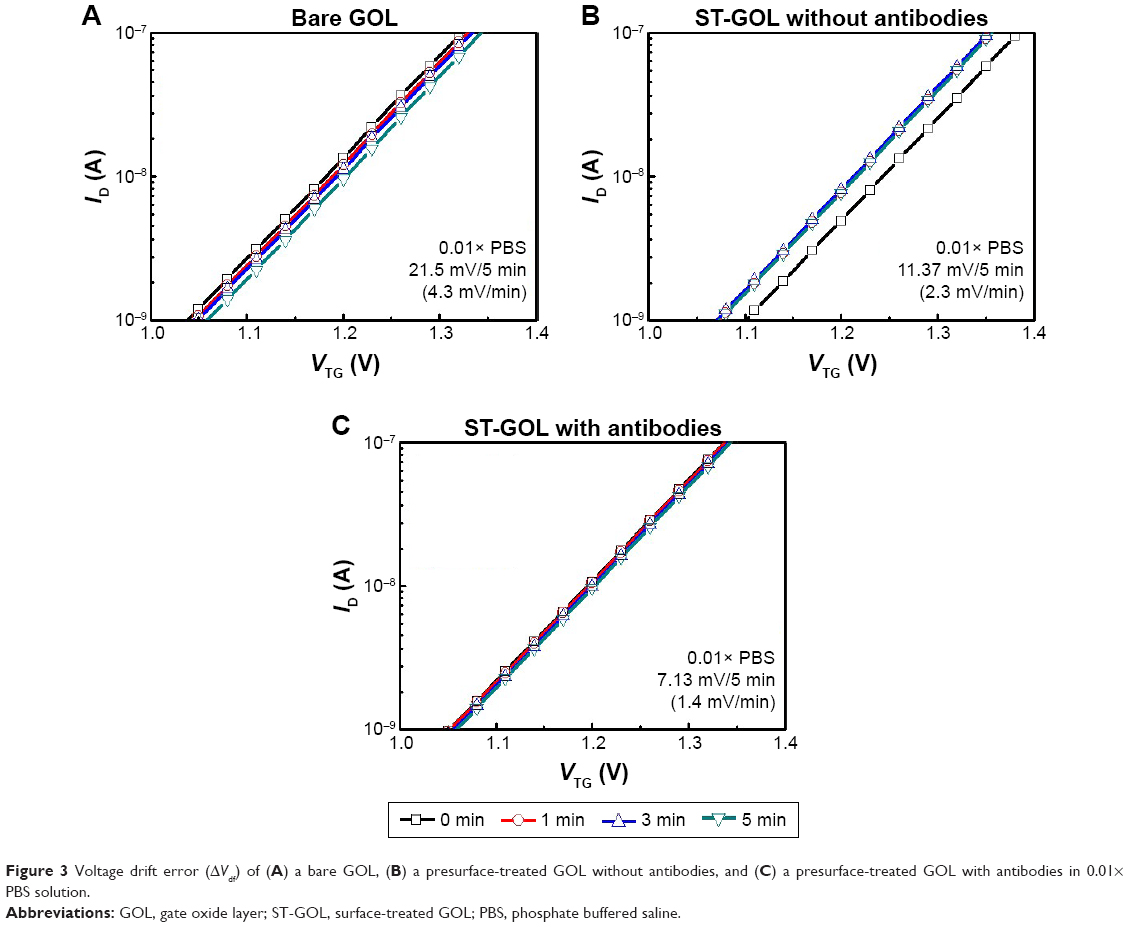 | Figure 3 Voltage drift error (ΔVdf) of (A) a bare GOL, (B) a presurface-treated GOL without antibodies, and (C) a presurface-treated GOL with antibodies in 0.01× PBS solution. |
An additional phenomenon that was observed was the consistent shift of the ΔVdf as time passes. This is because the nonpreconditioned GOL has an unstable surface and, thus, reacts with numerous ions of the PBS (OH−, H+, and O2−), for a long time. This phenomenon contributes to sensors being unable to produce reliable results when exposed to extended periods of testing.
In the cases of the ST-GOL without antibodies and the ST-GOL with antibodies, the ΔVdf values were significantly reduced. The ST-GOL without antibodies showed a ΔVdf of 11.37 mV/5 min (2.3 mV/min), and the ST-GOL with antibodies showed a ΔVdf 7.13 mV/5 min (1.4 mV/min). These values are only 19.2% of the Nernst limit and 12% of the Nernst limit, respectively. The reasons for the decreased ΔVdf can be thought to be due to the following. First, the random chemical reactions between the chemical links on the surface of GOL and ions of the PBS were restricted by the presurface treatment. Second, the number of residual chemical links that can react and bind to the ions within the PBS is limited and this causes saturation to occur very quickly.
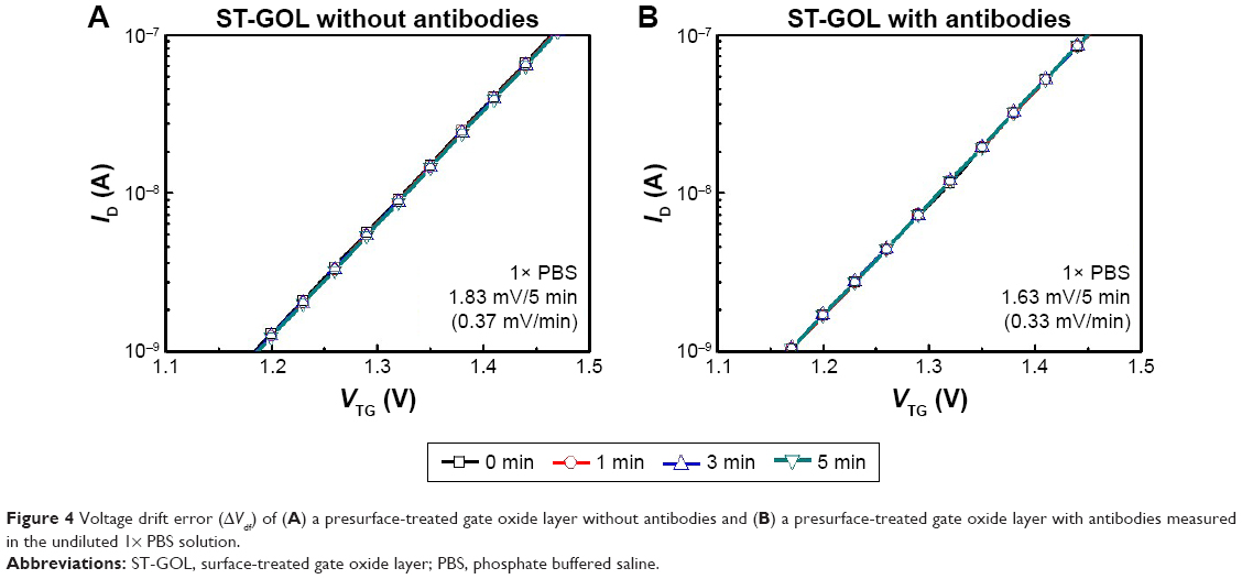
Figure 4A and B shows the ΔVdf values of adding undiluted 1× PBS solution to an ST-GOL without antibodies and to an ST-GOL with antibodies. The experiment was conducted under the same conditions as the experiment of Figure 3. As can be seen from the results, the ΔVdf results are much smaller than the ΔVdf of its 0.01× PBS counterpart: the ST-GOL without antibodies has a ΔVdf of 0.37 mV/min and the ST-GOL with antibodies has a ΔVdf of 0.33 mV/min. The significant reduction of the ΔVdf values is because of the Debye screening length in the 1× PBS. The 1× PBS has the much smaller Debye screening length of 0.7 nm than 0.01× PBS’s Debye screening length of ~7.3 nm.21,22 Consequentially, the GOL can only detect much smaller ions in 1× PBS, and as a result, the chemical reaction is rapidly saturated (or stabilized).
 | Figure 4 Voltage drift error (ΔVdf) of (A) a presurface-treated gate oxide layer without antibodies and (B) a presurface-treated gate oxide layer with antibodies measured in the undiluted 1× PBS solution. |
Figure 5 shows the results for all GOL ΔVdf values that were measured at the 0, 1, 3, 5, 10, 15, and 20 min marks in 1× PBS. For the bare GOL, the chemical links of the SnO2 surface reacted continuously with the ions in the PBS and the ΔVdf increased as time passed. This result is consistent with our past experiment. However, GOL that has undergone presurface treatment showed complete saturation by the ions in 1× PBS by the 1 min mark. Consequently, a presurface-treated GOL utilizing 1× PBS can decrease the noise from unwanted ions and produce a reliable biosensing signal.
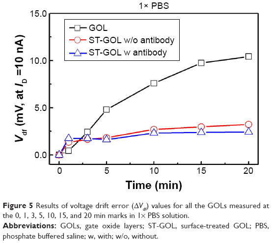 | Figure 5 Results of voltage drift error (ΔVdf) values for all the GOLs measured at the 0, 1, 3, 5, 10, 15, and 20 min marks in 1× PBS solution. |
The results clearly indicate that in scenarios where the ISFET is used to sense biomarkers, the undiluted 1× PBS could produce trustworthy biosensing signals. However, the 1× PBS will lead to a much shorter Debye screening length and subsequent biomarker detection limit. This can lead to problems if a lengthy or bulky bioconjugate, such as whole antibodies, is utilized. To solve the problem from the short Debye screening length, small capture linkers, such as antibody fragments, aptamers, and peptides, could be used instead of large whole antibodies.
Conclusion
This study used SnO2 as a gate oxide sensing layer in an ISFET biosensor to capture biomarkers and analyze their biosignals. The results demonstrate that proper surface treatment of a gate oxide sensing layer in an ISFET can significantly reduce the sensing signal error. Because the amounts of biomarkers in samples are usually minuscule, a biosensor must be sensitive enough to detect these biomarkers at low concentrations. To produce a longer Debye screening length for the ISFET biosensor, the sample media, which were the PBS solutions in this study, are diluted. However, this could lead to a situation where the media itself can cause both a large ΔVdf and a large margin of error, thus making the resulting biosensing signal unreliable. To decrease such error from the media, a more concentrated medium, such as 1× PBS, is utilized. The 1× PBS medium quickly reacts and saturates the surface of sensing gate and subsequently stabilizes the electrical potential. An unfortunate side result from adding the concentrated medium is the shortening of the Debye screening length. To overcome this obstacle, aptamers, peptides, and antibody fragments and immobilization materials that are shorter than a whole antibody need to be utilized to maintain a reliable sensor sensitivity outcome.
Acknowledgment
This study was supported by the Bio & Medical Technology Development Program of the NRF funded by the Korean government MSIP (2015M3A9E2029265) and Korea Health Technology R&D Project through the Korea Health Industry Development Institute (KHIDI) funded by the Ministry of Health & Welfare, Republic of Korea (HI15C-3078-020015).
Disclosure
The authors report no conflicts of interest in this work.
References
Bergveld P. Development of an ion-sensitive solid-state device for neurophysiological measurements. IEEE Trans Biomed Eng. 1970;17(1):70–71. | ||
Pablo Diniz B. An embedded measurement system for the electrical characterization of EGFET as a pH sensor. Meas Sci Technol. 2014;25(2):027001. | ||
Lee C-S, Kim KS, Kim M. Ion-sensitive field-effect transistor for biological sensing. Sensors. 2009;9(9):7111–7131. | ||
Jung-Chuan C, Pik-Kwan K, Zhi-Jie C. SnO2 separative structure extended gate H+-ion sensitive field effect transistor by the sol–gel technology and the readout circuit developed by source follower. Jpn J Appl Phys. 2003;42(11):6790–6794. | ||
Liao H-K, Chou J-C, Chung W-Y, Sun T-P, Hsiung S-K. Study of amorphous tin oxide thin films for ISFET applications. Sens Actuators B Chem. 1998;50(2):104–109. | ||
Jang H-J, Ahn J, Kim M-G, et al. Electrical signaling of enzyme-linked immunosorbent assays with an ion-sensitive field-effect transistor. Biosens Bioelectron. 2015;64:318–323. | ||
Lee IK, Jeun M, Jang HJ, Cho WJ, Lee KH. A self-amplified transistor immunosensor under dual gate operation: highly sensitive detection of hepatitis B surface antigen. Nanoscale. 2015;7(40):16789–16797. | ||
Batista PD, Mulato M. ZnO extended-gate field-effect transistors as pH sensors. Appl Phys Lett. 2005;87(14):143508. | ||
Leistiko O. The selectivity and temperature characteristics of ion sensitive field effect transistors. Phys Scr. 1978;18(6):445–450. | ||
Schöning MJ, Tsarouchas D, Beckers L, et al. A highly long-term stable silicon-based pH sensor fabricated by pulsed laser deposition technique. Sens Actuators B Chem. 1996;35(1):228–233. | ||
Bousse L, van den Vlekkert HH, de Rooij NF. Hysteresis in Al2O3-gate ISFETs. Sens Actuators B Chem. 1990;2(2):103–110. | ||
Liu BD, Su YK, Chen SC. Ion-sensitive field-effect transistor with silicon nitride gate for pH sensing. Int J Electron. 1989;67(1):59–63. | ||
Rocher V, Poyard S, Jaffrezic-Renault N, Ajoux C, Lemiti M, Sibai A. Photo-CVD silicon nitride thin layers as pH-ISFET sensitive membrane. Sens Actuators B Chem. 1994;19(1):342–347. | ||
Poghossian AS. The super-Nernstian pH sensitivity of Ta2O5-gate ISFETs. Sens Actuators B Chem. 1992;7(1):367–370. | ||
Jung Chuan C, Lan Pin L. Study of TiO2 thin films for ion sensitive field effect transistor application with RF sputtering deposition. Jpn J Appl Phys. 2004;43(1):61–65. | ||
Chou JC, Chiang JL. Study on the amorphous tungsten trioxide ion-sensitive field effect transistor. Sens Actuators B Chem. 2000;66(1–3):106–108. | ||
Watson J, Ihokura K. Gas-sensing materials. MRS Bull. 1999;24(6):14–17. | ||
Sohn Y-S, Lee YK. Site-directed immobilization of antibody using EDC–NHS-activated protein A on a bimetallic-based surface plasmon resonance chip. J Biomed Opt. 2014;19(5):051209. | ||
Sarkar D, Liu W, Xie X, Anselmo AC, Mitragotri S, Banerjee K. MoS2 field-effect transistor for next-generation label-free biosensors. ACS Nano. 2014;8(4):3992–4003. | ||
Knopfmacher O, Tarasov A, Fu W, et al. Nernst limit in dual-gated Si-nanowire FET sensors. Nano Lett. 2010;10(6):2268–2274. | ||
Elnathan R, Kwiat M, Pevzner A, et al. Biorecognition layer engineering: overcoming screening limitations of nanowire-based FET devices. Nano Lett. 2012;12(10):5245–5254. | ||
Stern E, Wagner R, Sigworth FJ, Breaker R, Fahmy TM, Reed MA. Importance of the Debye screening length on nanowire field effect transistor sensors. Nano Lett. 2007;7(11):3405–3409. |
 © 2017 The Author(s). This work is published and licensed by Dove Medical Press Limited. The full terms of this license are available at https://www.dovepress.com/terms.php and incorporate the Creative Commons Attribution - Non Commercial (unported, v3.0) License.
By accessing the work you hereby accept the Terms. Non-commercial uses of the work are permitted without any further permission from Dove Medical Press Limited, provided the work is properly attributed. For permission for commercial use of this work, please see paragraphs 4.2 and 5 of our Terms.
© 2017 The Author(s). This work is published and licensed by Dove Medical Press Limited. The full terms of this license are available at https://www.dovepress.com/terms.php and incorporate the Creative Commons Attribution - Non Commercial (unported, v3.0) License.
By accessing the work you hereby accept the Terms. Non-commercial uses of the work are permitted without any further permission from Dove Medical Press Limited, provided the work is properly attributed. For permission for commercial use of this work, please see paragraphs 4.2 and 5 of our Terms.